if this is not right place for this topic, I'm sorry. I'm new to diyAudio and this is the first post. My experience in electronic design is close to zero, there is only basic knowledge.
There are a lot of threads regarding this, but i was not able to find a decision.
My plan is: building a up to 8 Chanel pre-Amp proto with this chain:
4xSpdif in -> I2S->Adau1701 ->(up to) 4xDAC -> Volume IC -> preAmp/Buffer -> RCAout
Parts:
Spdif in -> unclear
Adau1701 ->Wondom APM2
DAC ->PCM1502( maybe upgrade later)
Volume -> PT2258
preAmp/Buffer -> update 23.01.2025 from youtube channel "Franks Werkstatt der Lautsprechertechnik"
uC for Control -> not sure
Input sample rate: 44,1kHz.
At the moment i am working/struggling on I2S distribution, I2S input (with MCLK) comes from Arylic pro V3, output is Adau1701 Dac for debugging and a PCM5102 I2S Dac board.
APM2 is working as slave (MCLK in) with 16Bit output. All signals visible on scope.
1.) BCLK and LRCLK wired simply parallel to Arylic, PCM5102, Adau xCLKin and Adau xCLKout --> Adau DAC works, PCM5102 works not
2.) changed to 100Ohm in series at Arylic BCLK and LRCLK --> outputs are working, but some clitching noises every 10- 20s also on booth outputs
3.)resistor changed to 50Ohm --> same as no 2, but with much more noise
The Signals of Data in/out and LRCK looking good, in my opinion, but BCLK get more worse with each additional I2S connection. Because of the target to have up to 4 IS2 DACs, i think it is not solvable wit some Rs and Cs.
So, i want to buffer the signals with 74hc125, one behind I2S in and second behind APM2. To prevent timing problems all signals should be buffered also MCLK and DataIn/out. Good Idea or bad? Is one buffer able to drive 4 of these dacs, or ist better to use more buffers?
grateful for any critics, hints or opinions
Last edited:
4x spdif should give 4x I2S bitstreams that need to be routed directly to ADI or whatever processor you're using, not sure what you're looking to split / distribute.
oh, sorry, maybe it is not described well, because of my englisch skills.
planned is just one spdif->i2s input stream, 4xspdif should be realized by an 4to1 input selector.
I want to distribute the BCLK ,LRCK ,(MCLK) comming form Arylic pro V3( I2S master), to the DSP board and 4 I2S Dacs. At the moment on breadboard i have only one DAC, and have 4 wires connected at BCLK and LRCLK (Arylic, DSPin,DSPout; DACin). The signal quality, mainly BCLK, looks not good. But the target is to have 4 DACs --> 3 additional lines for each clock .
The problem that i have, is to improve the signal quality. So i had ordered some 74hc125 as I2s buffers. Some hints or help would be nice.
BTW: idea to realize 4x spdif input selector is also using 74hc125, just by switching the ic ouputs on and off. Good or Bad?
Clock buffer.want to distribute the BCLK ,LRCK ,(MCLK) comming form Arylic pro V3( I2S master), to the DSP board and 4 I2S Dacs.
BTW: idea to realize 4x spdif input selector is also using 74hc125, just by switching the ic ouputs on and off. Good or Bad?
Works only for TOSLINK. Coaxial SPDIF is 0.5Vpp and needs to be switched using an analogue MUX like HC4051.
Thanks, i will add one of the breakout boards to my buying list, to play around.Only over TOSLINK. Coaxial SPDIF is 0.5Vpp and needs to be switched using an analogue MUX like HC4051.
Some opinion where to buffer, imo I2Sin (after arylic) all lines. Should i use 1 buffer for all DACs or 1 buffer for each?
One each, preferably on the same chip, like HC245 (8 lines).
And do not use breakout boards, have a properly designed PCB with a ground plane or nothing will work well. Remember that your setup is already compromised (jitter-wise) due to the buffering of I2S lines.
And do not use breakout boards, have a properly designed PCB with a ground plane or nothing will work well. Remember that your setup is already compromised (jitter-wise) due to the buffering of I2S lines.
Last edited:
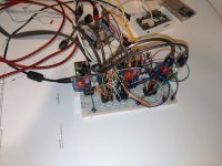
Today the HC125 will arrive. Will be 5 pcs. of it, so hopefully they not rubbish for some experiments, but they have just 4 lines.
Maybe later on i will post a pic that explains what i mean.
Thanks for input, very happy about it
Unfortunately, i had never designed a pcb, thats the point i want to change. My Plan is to design something like a backplane, with connectors for DAC, mounted DSP, power supply/distribution, buffering .... Full digital, no analog signals on it.And do not use breakout boards, have a properly designed PCB with a ground plane or nothing will work well.
Maybe later on i will post a pic that explains what i mean.
Thanks for input, very happy about it
Hi,
it works, no distorting sound or something else.
I had needed all 5 pcs of HC125, because of the signal quality from the arylic pro and sure dsp. Setup is now.
IIS(Arylic) --> Buf --> DSP -->Buf -->3xBuf-->3xDAC
The Arylic is realy sensitive to any load on the IIS output, and reacts different depending the the selected source of the arylic (have look in arylic forum). Adding a buffer, improved the signal very well, independent from selected source. The buffer should decouple also other IIS sources, additional it does also level shifting from 5V if needed.
The sure dsp is similar, very sensitive to different loads, if you want to have not just point to point connection, you will probably run into problems. --> Buf after DSP decouples load.
Each DAC has its own BUF, to decouple DAC load from signal distribution. To give the possibility to change to other DAC type and do not think about its load.
During my experiments, i had observed that 1 HC125 can drive all 4 DAC HC125 Buf without effecting signal quality, without any resistors in series. I have tried some series resistors and it worsen the the signal each time. Maybe this is the reason of the sensitivity of the arylic and sure, they have R in series. With additional R and C, tau increases and worsen your signal edge.
Outcome is basically i will go on with this solution, the buffer after DSP should be changed to HC254 to have more data lines.
Should i build up an experimental board above or should i start directly to create my first correct circuit board. I als o need to design a power supply solution.
Attachments
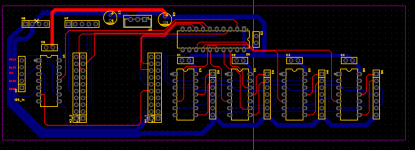
This is my first attempt at designing a circuit board. It has 4 layers, layer 2 is DGND, layer 3 is AGND, the grounds are not connected to separate analog and digital part of used DACs. Is this good/bad Idea?
On the breadboard solution form above, i did not use any R. Does it makes sense, to add some 0Ohm R's to the CLK/Data-Lines, that makes it possible to change the resistors later on?
I would be happy about some some help, to improve the mistakes and rubbish things in this design.
On the breadboard solution form above, i did not use any R. Does it makes sense, to add some 0Ohm R's to the CLK/Data-Lines, that makes it possible to change the resistors later on?
I would be happy about some some help, to improve the mistakes and rubbish things in this design.
Attachments

Do not do that, always use some 100 ohms in series. The quality you "see" on your scope is not very valid since scope capacitance is typically 25pF with the typical logic input only around 3-5pF.During my experiments, i had observed that 1 HC125 can drive all 4 DAC HC125 Buf without effecting signal quality, without any resistors in series. I have tried some series resistors and it worsen the the signal each time. Maybe this is the reason of the sensitivity of the arylic and sure, they have R in series. With additional R and C, tau increases and worsen your signal edge.
Thanks newvirus.
You are right, my scope has 15pF and is a simple 50Mhz Rigol, absolutely possible.
here is the revised version.
1. resistors added to each clock and data line, not behind the output buffers
2. possibility to choose for common 5V input voltage, or seperate for DSP, to have possibility for different power up sequences
3. connection point for AGND and DGND
4. Leds added for debugging and create min load
Feel free to roast me.
Last edited:
On the Input section of my build i would like to have an ADC in slave mode, so i would like to ask, how to buffer. The clock signals are going to the ADC and data line is coming from ADC,. In my opinion this will end up in 2x buffer time delay between clock and data lines. How can i solve this problem.
The hole pre amp should be controlled by teensy 4, it will be also used for SPDIF to I2S conversion, the ADC should also be connected to the teensy board I2S in. Dircet connection is simply possible, but connection with buffer???
The hole pre amp should be controlled by teensy 4, it will be also used for SPDIF to I2S conversion, the ADC should also be connected to the teensy board I2S in. Dircet connection is simply possible, but connection with buffer???
It is alive and it plays!
.
 There where no audible noises, like plops and so on, during the first test. I am happy. Never the less, i have to do some more testing for example the I2C connection to the APM2 board. The measurements of the output signal like THD is only possible by REW for me, for measuring jitter i don't have any idea with my equipment. Are there any suggestions to measure this and hints for further improvements of the board.
The resistors before output buffers are 100Ohm, all others in the signal lines are 22Ohms. I did one fail, the footprint of the LM1117 is turned upside town, so i had to mount the regulator "the wrong direction"
.
The resistors before output buffers are 100Ohm, all others in the signal lines are 22Ohms. I did one fail, the footprint of the LM1117 is turned upside town, so i had to mount the regulator "the wrong direction"

Yes, it is 4 Layer, and 2nd and 3rd are ground planes, analog GND and digital GND. By default they are not connected, it is connectable by Jumper (H9).
I did some measurments, with the board and the 3 mounted dacs, the THD Measurement where done by simple loop from built in PC sound card from line out to line in. This not precise, but the best i have in my hobby room. So i compare the results relatively, to the absolute Values i do not trust. Power source was a old K2612 SMU.
Power Consumtion @5V, with 3Dacs and 1kHz signal at 0dBFs = ~210mA
Distortion direct loop 1kHz 1Vrms

Dac with voltage devider 0.5 at outputs direct connected to source (arylic pro)

Dac with voltage devider 0.5 at outputs mounted on the board 0dbFS:

The power distribution was connected vie bread board, i had the feeling this was also influencing the THD value.
Pleas give feedback. what you think.
Power Consumtion @5V, with 3Dacs and 1kHz signal at 0dBFs = ~210mA
Distortion direct loop 1kHz 1Vrms
Dac with voltage devider 0.5 at outputs direct connected to source (arylic pro)
Dac with voltage devider 0.5 at outputs mounted on the board 0dbFS:
The power distribution was connected vie bread board, i had the feeling this was also influencing the THD value.
Pleas give feedback. what you think.
Are there any suggestions to measure this and hints for further improvements of the board.
THD etc. shouldn't be an issue as your loudspeaker already has more distortion than anything else in the signal chain.
It is best to not attempt measuring small quantities of jitter. The buffer ICs probably added less than 100ps.. Just let it go and enjoy the music....for measuring jitter i don't have any idea with my equipment.
Yes, but also the DAC board is not the leading edge one, i will go forward with the integration with the rest of the pre amp. I would also like to thank you, your inputs where very helpful and the goal is mainly reached, besides untested I2C function.THD etc. shouldn't be an issue as your loudspeaker already has more distortion than anything else in the signal chain.
After connecting the board to the preamps and simple chip amp, some experiments where done. At switch on/off, no noises or plobs where heard, not only with main power also by plug bread board cables in and out. Not playing music and volume max --> silence, nothing. Also music sounds not bad, better than computer onboard sound.
Next step is to add the PT2258 Volume controller, to implement the Teensy and Power distribution.
Last edited:
- Home
- Design & Build
- Electronic Design
- ADAU1701 Pre-Amp I2S distribution