Hi all,
I am in need of finding a way of converting a single-ended signal to differential - input to an ADC, yet without having to use opamps and also preferably without using additional circuitry. I hope one of you have a good idea for this ... 😉
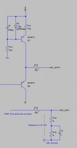
I have attached a schematic illustrating what the driver-to-ADC interface looks like. What is needed is a way to "lift" the "previous circuitry ground" to 2.5 VDC so that it centers around the Vref of the ADC. Normally, this could be done using opamps but I'd prefer to not use an opamp or more circuitry. I've been thinking of maybe a couple of resistors (making a voltage divider connecting to the previous ground) with a capacitor to stabilize the potential but maybe there's a better way?
I'd appreciate your insights 😉
Cheers,
Jesper
I am in need of finding a way of converting a single-ended signal to differential - input to an ADC, yet without having to use opamps and also preferably without using additional circuitry. I hope one of you have a good idea for this ... 😉
I have attached a schematic illustrating what the driver-to-ADC interface looks like. What is needed is a way to "lift" the "previous circuitry ground" to 2.5 VDC so that it centers around the Vref of the ADC. Normally, this could be done using opamps but I'd prefer to not use an opamp or more circuitry. I've been thinking of maybe a couple of resistors (making a voltage divider connecting to the previous ground) with a capacitor to stabilize the potential but maybe there's a better way?
I'd appreciate your insights 😉
Cheers,
Jesper
Attachments
Be careful here, most of the ADC parts are charge transfer delta sigma meaning they need a few nF of cap across the input to provide the charge for the acquisition phase, you then need a driver stiff enough to drive this cap.
This is somewhere where something opamp like is very much the easiest way, some sort of totem pole output driving each leg with feedback jiggered to make it stable into a few nF.
The guys designing these chips designed them to be driven by an opamp like output (via a few tens of ohms to isolate the required cap), and they are somewhat sensitive to how you drive them if you want to get anywhere near the datasheet numbers.
Ref the DC bias thing, check the data sheets but it may be that you can simply do a series cap with a reasonably high value resistor to the common mode voltage pin....
One other thing to watch is abs max ratings on the analogue inputs, particularly with regard to startup and other such transient events, clamp diodes are a good idea.
Regards, Dan.
Hi Dan,
& thanks for your elaborate answer ;-)
Actually, I am aware of the capacitor & drive specifications for the ADC (clamp diodes, series resistor value, capacitor value) but would like to omit the opamps if I can. Unfortunately the datasheet has no information on this - except for using opamps - so I getting a good idea about how to do this would be attractive ... To that end ... I'm not quite sure what you mean by this:
Cheers,
Jesper
P.S.: I just realized that the schematic I attached had an error regarding connecting the resistor network and capacitor. New one attached ...
& thanks for your elaborate answer ;-)
Actually, I am aware of the capacitor & drive specifications for the ADC (clamp diodes, series resistor value, capacitor value) but would like to omit the opamps if I can. Unfortunately the datasheet has no information on this - except for using opamps - so I getting a good idea about how to do this would be attractive ... To that end ... I'm not quite sure what you mean by this:
Do you suggest that I connect a resistor to the ADC's Vref and then in series with this resistor a capacitor to the ADC ground?Ref the DC bias thing, check the data sheets but it may be that you can simply do a series cap with a reasonably high value resistor to the common mode voltage pin....
Cheers,
Jesper
P.S.: I just realized that the schematic I attached had an error regarding connecting the resistor network and capacitor. New one attached ...
Attachments

Last edited:
You need to fix the ADC- input at half the input voltage at low impedance, like the circuit at the ADC+ input, but just with a fixed voltage divider.
Most ADC chips require very low impedance driver and also require a large capacitor at the input.
And not to forget, you loose 6 db S/N ratio by not running the input differential and most ADC chips will also get reduced performance on t.ex. THD.
Most ADC chips require very low impedance driver and also require a large capacitor at the input.
And not to forget, you loose 6 db S/N ratio by not running the input differential and most ADC chips will also get reduced performance on t.ex. THD.
You need to fix the ADC- input at half the input voltage at low impedance, like the circuit at the ADC+ input, but just with a fixed voltage divider.
Most ADC chips require very low impedance driver and also require a large capacitor at the input.
And not to forget, you loose 6 db S/N ratio by not running the input differential and most ADC chips will also get reduced performance on t.ex. THD.
Hi Søren,
Thanks for your feedback and comments. Hmmm ... looking at ADC data sheets I have noted the low impedances and often relatively high capacitances on their inputs. I take it this takes some experimentation to find an optimum value for input capacitance and impedance.
I'm also aware of the reduced SNR but was hoping to maybe get around the reduced THD specs by loading the two ADC differential inputs in a similar way so that they don't really "know" that it's a single-ended amplifier.
You need to fix the ADC- input at half the input voltage at low impedance, like the circuit at the ADC+ input, but just with a fixed voltage divider.
Thanks for the tip: Would that be to make a copy of R15 & R16 in the schematic in #3 and place it similarly on the ADC_DIFF+ input? And then eliminate C9 (which would short the signal to ground)?
BTW - good luck with your DAM DAC ;-)
Cheers,
Jesper
It would be easier to use a differential opamp like OPA1632:
http://www.ti.com/lit/ds/symlink/opa1632.pdf
Passive solution would be to use a x:1+1 transformer with Vcom connected to secondary center tap.
http://www.ti.com/lit/ds/symlink/opa1632.pdf
Passive solution would be to use a x:1+1 transformer with Vcom connected to secondary center tap.
Hi Søren,
Thanks for the tip: Would that be to make a copy of R15 & R16 in the schematic in #3 and place it similarly on the ADC_DIFF+ input? And then eliminate C9 (which would short the signal to ground)?
Like exactly the same, including the transistor, you need the low impedance.
And then fix the input to AC ground. Would help if you showed all of your input circuit....
Capacitors then as per ADC manufacturers recommendation.
@mhelin: Thanks for suggesting but in the first round I'd prefer to stay with the single-ended solution ... 😉
@soekris: I've attached a copy of the schematic which shows the circuitry going to the ADC - not yet completed but currently it looks like this. In this I've included what I reckon are your suggestions (?) - hope I understood it correctly ...
What I've understood from elsewhere is that as long as the input impedances to both the ADC+ & ADC- inputs are identical & match with what is optimum for the ADC (as per the manufacturer) then it should be fine. To that end I intended to make precise measurements of the output impedances of the emitter follower on ADC+ so as to match (schematic in post #1):
- the output impedance of the emitter follower + R13 to ...
- the value of R14.
Thus, the input impedances to ADC+ & ADC- would be the same on the ADC+ & ADC- inputs. However, if I understood you correctly you would suggest something akin to the schematic attached to this post?
Don't know how it is in your part of the country but here there's a fine white layer of snow most everywhere (like it - but I don't have to drive 🙄)
Cheers,
Jesper
P.S.: the GND going into ADC- in the schematic in post #1 is the ground coming from the preamp circuitry so it already IS low impedance ...
Attachments
Last edited:
Just connect the Vcom (or Vref/2 depends on ADC what kind of reference / common voltage level is available) to ADC- and signal to ADC+ (coupled by a capacitor).
Last edited:
I am in need of finding a way of converting a single-ended signal to differential - input to an ADC...
may not really be the best conceptualization - you have a ADC with diff input
and a "signal" voltage which is always a voltage difference between 2 circuit nodes
all signals, even single ended, always have a reference
so you need a way to connect the 2 nodes representing the signal difference to the ADC differential input
preferably with no loss or distortion in your signal bandwidth and meeting the ADC input operating requirements
if you need DC offset then use 2 big caps to AC couple both of the signal's nodes ,"hot" and "gnd", to the ADC +,- inputs
if you buffer with EF then you want the same Z, same DC offsets (number of, direction of Vbe drops), same divider relation for each of signal hot and gnd to the respective ADC inputs
you could share the V ref in your current sources to gain a little noise performance from the ADC common mode rejection
and in the ccs it is very "inefficient" to bypass the low Z of the reference LEDs with the big elelctros - usually better to split the LED bias pull down R and make a filter with the center node and the big cap to the rail the LED is referenced from to reject supply noise in the LED bias
usually the LED will quiet enough on its own but if more LF noise reduction is needed then make another low pass filter with an explicit ~100 Ohm resistor from the LED to the Q base and the big cap
Last edited:
Hi all - once more thanks for your replies ... ;-)
@jcx: Very informative & useful feedback, jcx - thanks.
I think I mostly understand what you are saying although I'm not quite clear about what you mean with "to split the LED bias pull down R". This R would it be e.g. R11 or R12 in the top CCS of post #9?
About inserting a 100 ohm resistor inbetween the LED and the Q base ... I see your point but in this design I'm trying to obtain an overall very low LF noise and the HLMP-6000 LED - which I'm intending to use - has a dynamic impedance of about 8 ohms (measurement courtesy Samuel Groner). And since even a 3300 uF low impedance electrolytic (to my knowledge) can have a substantial impedance at low frequencies I was thinking that the LED would have a lower impedance at very LF than a series resistor ....
@TNT:
I haven't decided yet but it seems to me that all the potentially superb ADCs have a differential input - so I have to find a solution to this "single-ended to differential interface".
@mhelin: Thank you also for suggesting - but as I'm also intending to omit any capacitors in the direct signal path I need to find another solution ...
Cheers,
Jesper
@jcx: Very informative & useful feedback, jcx - thanks.
and in the ccs it is very "inefficient" to bypass the low Z of the reference LEDs with the big elelctros - usually better to split the LED bias pull down R and make a filter with the center node and the big cap to the rail the LED is referenced from to reject supply noise in the LED bias
usually the LED will quiet enough on its own but if more LF noise reduction is needed then make another low pass filter with an explicit ~100 Ohm resistor from the LED to the Q base and the big cap
I think I mostly understand what you are saying although I'm not quite clear about what you mean with "to split the LED bias pull down R". This R would it be e.g. R11 or R12 in the top CCS of post #9?
About inserting a 100 ohm resistor inbetween the LED and the Q base ... I see your point but in this design I'm trying to obtain an overall very low LF noise and the HLMP-6000 LED - which I'm intending to use - has a dynamic impedance of about 8 ohms (measurement courtesy Samuel Groner). And since even a 3300 uF low impedance electrolytic (to my knowledge) can have a substantial impedance at low frequencies I was thinking that the LED would have a lower impedance at very LF than a series resistor ....
@TNT:
May I ask wich ADC you are discussing?
I haven't decided yet but it seems to me that all the potentially superb ADCs have a differential input - so I have to find a solution to this "single-ended to differential interface".
@mhelin: Thank you also for suggesting - but as I'm also intending to omit any capacitors in the direct signal path I need to find another solution ...
Cheers,
Jesper
the opamp mentioned by Mhelin is in my humble opinion a much better solution than the non-linear drive capacity of an emitter follower. the input noise is specified at a gain of +1 (!), quite a remarkable performance. the adc expects a stiff source, stiff up to several Mhz, (helped with capacitors at the input).
What drives the requiremnt to have low source impedance as such high frequency?
btw I'm bulidng the Acko ADC with an ESS chip.
//
btw I'm bulidng the Acko ADC with an ESS chip.
//
the switched capacitor input sampler needs to settle fast. that´s why a relative large input paralell capacitor is stabilizing the audio signal at the oversample frequencies
Basreflex: You seem to have insight in the matter. Could you point to some litterature that you would suggest valuable to read?
//
//
@mhelin & basreflex: There are so many ways in audio ;-) Yet my interest right now is to find a way to connect this single-ended signal to a differential ADC in the - hopefully - best possible way - resembling a single-ended signal. But thanks for considering.
@TNT: In the ES9102 datasheet (available from ismosys by signing an NDA) it is indicated how the ES9102 is optimally connected to the exterior. And, to that end, if you are interested in using opamps, Samuel Groner some years ago made an extensive investigation into various opamps e.g. the OPA2134. The paper is available here:
SG-Acoustics · Samuel Groner · IC OpAmps
However, his paper does not include the newer opamps like e.g. LME49990 or the like.
Best regards,
Jesper
Last edited:
- Status
- Not open for further replies.
- Home
- Source & Line
- Digital Line Level
- Adapting a single-ended signal to ADC.