Thanks darkfenriz, I thought it is some kind of protection, but I can't figure out the mechanism of it, could you elaborate it a bit further?
As far as I understand the circuit:
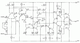
-at normal operation, both Q50 and Q64 are kept below threshold Vbe
-Q19 and I3 form the main, final VAS
-collector of Q17 drives the Q18 buffer and this drives Q19 VAS
- at positive overload Q17 collector to I3 upper node voltage gets high, here Q64 starts to conduct
- at negative overload Q50 conducts
I understand it as two anti-parallel diodes at current mirror.
Regards
Adam
- Status
- Not open for further replies.