Thanks for the advice, I will work the problem again in the weekend.
I have tried cooling every component when warm (with cold spray), with no results, but have not tried applying heat selectively to cold components.
Yesterday I tried replacing R6, R6, R14, R15 (around the DC trimpot), to rule out any thermal issues with these, but it didn't help. So will put the original resistors back, and move to the next "suspects" around the input transistors..
So... I still haven't been able to find the cause of the DC drift issue, and I have run out of things to try:
Since last post, I have replaced all the resistors around the Q1, Q2 and Q3 to rule out any thermal issues or excessive drift. Didn't make any difference.
All transistors and diodes on the board have been replaced either by new devices, or swapped over from the good channel.
Exception: Q1, the input JFET pair, have just been rotated 180, to see if that changed the polarity of the DC offset - which it didn't.
Everything seems to measure correctly, from Q1 up to the bases of the drivers (Q12/13), were the unbalanced voltages appear.
The two symmetrical pairs (Q2/Q3) are evenly matched both when cold and warm. In other words: The DC offset probem does not come from the input section.
Question is then: Where DOES it come from??
When everything is nicely balanced and even all the way up to the Q6/Q7 Collectors, what can possibly cause a DC drift of more than +1.2V from cold to warm? (the amp DC protection circuit kicks in at this level).
It takes about an hour for the DC offset to get over 1 volt, when the amp is turned on cold with DC offset around zero.
I have several times tried using cooling spray on every single component, but have not been able to get the DC offset to drop again with this method.
I don't know what else to try now, so would really appreciate some good advice.. Thanks in advance.
Without re-reading everything, did you check the resistors also,
for instance with a method like suggested in post 20 ? Can you
add a good close up picture of the board ?
for instance with a method like suggested in post 20 ? Can you
add a good close up picture of the board ?
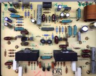
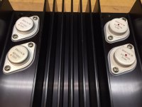
Hi, yes all resistors have been (triple) checked, and the resistors around the input pairs are now new (Yageo 1% film) - as you can also see from the pictures attached here.
The only original transistor left is the Q1, which has even Source voltages both cold and warm (around 100mV, which is the same as the good channel).
Don't know if I mentioned it earlier, but the other (good) channel only drifts about 50mV from cold to warm - just for comparison.
The only original transistor left is the Q1, which has even Source voltages both cold and warm (around 100mV, which is the same as the good channel).
Don't know if I mentioned it earlier, but the other (good) channel only drifts about 50mV from cold to warm - just for comparison.
Attachments
Do you own a lcr tester ?
Ebay "LCR-T4 Mega328 Transistor Tester" and similar are cheap and very useful for
passive and semiconductor parts.
I had difficulties with brown caps in Accuphase gear two times like those in your pics. .
Ebay "LCR-T4 Mega328 Transistor Tester" and similar are cheap and very useful for
passive and semiconductor parts.
I had difficulties with brown caps in Accuphase gear two times like those in your pics. .
I am leaning towards Q1 from higher gate leakage currents as the device warms up, because when you increased the dc NFB by adding the cap/cutting the dc path, the problem went away. I think maybe to test, remove the device, bias it and test the leakage of the gate cold and hot. The two gates see different resistances to ground so if the leakage goes up even by the same amount, the gate voltages imbalance.
I suspected Q1 also and suggested to reverse it (symmetrical pin out),
but the drift polarity did not change. Do you think this was probably a
thought error ? Not sure original poster swapped Q1 between channels.
but the drift polarity did not change. Do you think this was probably a
thought error ? Not sure original poster swapped Q1 between channels.
Last edited:
Regarding VR1: Yes, I put the original trimpot back when I replaced all the resistors around there. It works fine after cleaning, and the multiturn I had swaped in was not the correct value.
Hi mikeATX, you bring up a good point: "The two gates see different resistances to ground so if the leakage goes up even by the same amount, the gate voltages imbalance." - I had not considered that!
I think I will simply try and replace it either with a pair of SK117 (which I have), or swap in the SK150 from the other channel.
Yes I have a generic Mega328 tester, and a DER DE-5000 LCR meter and also a simply curve tracer - but that only works for BJT.
Correct, even if the devices are matched, if they both start leaking more as they heat up, the asymmetry in the dc paths will change the offset. This is similar to what happened to me with degraded beta in a bjt front end except the degradation was constant, and the trimpot could no longer correct for the imbalance.
The fault has been found..
Hello again, the fault has (finally) been found, and is was the most obvious suspect: The JFET input pair, 2SK150...
After replacing the dual JFET with two SK117, the DC offset stays stable (+/-10mV), and there is no drift after an hour. So that's great!
The SK117 I had, are not a good match though, so they still have to be replaced by a matched pair. I think I wil order 200 pcs SK209 (the SMD version), as these are available from Mouser, and use SOT>DIP adapter PCB.
So why didn't I just try replacing the 2SK150 (Q1) to start with? Well, I went down the wrong track because:
1. I couldn't measure any imbalance in the input stage. All the voltages around Q1, Q2, Q3 looked fine, and was equal to the other (good) channel.
2. The DC-offset didn't go down when using freeze spray on the 2SK150.
3. I desoldered it, and rotated it 180, so the JFET's switched position in the circuit. This didn't make any difference, so I concluded the 2SK150 was not the problem.
I think both point 2 and 3 above should reveal a fault, if it was just one side of the JFET pair that was leaky/unstable. But apparently, both sides of the JFET pair had about equal leakage, so the offset stayed the same. And I had overlooked the (basic) fact of the differences in Gate to ground resistance, that mikeAtx pointed out (thank you!).
So there are lessons to be learned here.
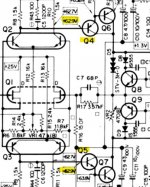
The question is then, what in-circuit measurements could I have made, that would have directly pointed to Q1 as the problem?
I think the DC-offset should be present on the bases of Q4/Q5, but measuring difference of 5-10mV is not easy here, as the nominal 62.9V fluctuate continously. But perhaps there is better way to check this?
Hello again, the fault has (finally) been found, and is was the most obvious suspect: The JFET input pair, 2SK150...
After replacing the dual JFET with two SK117, the DC offset stays stable (+/-10mV), and there is no drift after an hour. So that's great!
The SK117 I had, are not a good match though, so they still have to be replaced by a matched pair. I think I wil order 200 pcs SK209 (the SMD version), as these are available from Mouser, and use SOT>DIP adapter PCB.
So why didn't I just try replacing the 2SK150 (Q1) to start with? Well, I went down the wrong track because:
1. I couldn't measure any imbalance in the input stage. All the voltages around Q1, Q2, Q3 looked fine, and was equal to the other (good) channel.
2. The DC-offset didn't go down when using freeze spray on the 2SK150.
3. I desoldered it, and rotated it 180, so the JFET's switched position in the circuit. This didn't make any difference, so I concluded the 2SK150 was not the problem.
I think both point 2 and 3 above should reveal a fault, if it was just one side of the JFET pair that was leaky/unstable. But apparently, both sides of the JFET pair had about equal leakage, so the offset stayed the same. And I had overlooked the (basic) fact of the differences in Gate to ground resistance, that mikeAtx pointed out (thank you!).
So there are lessons to be learned here.
The question is then, what in-circuit measurements could I have made, that would have directly pointed to Q1 as the problem?
I think the DC-offset should be present on the bases of Q4/Q5, but measuring difference of 5-10mV is not easy here, as the nominal 62.9V fluctuate continously. But perhaps there is better way to check this?
Attachments
I think very hard to find, but easy too. In a way you followed the same path I did. Voltages looked ok near the input. But because of NFB and high gain from in to out, a small almost unmeasurable difference is going to cause a problem. So in the future, I'll probably just replace the input. Those devices are usually not that expensive anyway. So maybe easy in the future.
Well yes, but the problem is not the price of the parts, but that the JFET input transistors (often dual) from the good 70's and 80's amplifiers are simply no longer available. If I could just have ordered two new 2SK150A, I perhaps would have tried replacing them to begin with.
But it takes quite some time to research suitable replacement devices, and then find a place I can buy at least 100 pcs, in order to get a few well matched pairs. So not always so simple...
Do you agree that DC-offset due to leakage in Q1 should be measureable on Q4/Q5 (at least theoretically)? - also when taking into account the differences in Gate to ground resistance of Q1.
The happy ending..
So in the end, it was indeed the most obvious fault: Leaking JFET input pair.
I managed to make two quite well matched pairs of SK117 as replacement, with Idss 3.53/3.50 and 3.33/3.39, and replaced the dual JFET SK150A in both channels.
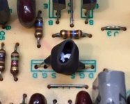
I mounted them face to face, and heatshrinked (see pic).
The result was very very good: From cold to warm (heatsinks around 40c), the DC offset now moves only 4-5mV! 😀
The "good" channel (which was working fine) had a drift of about 60mV with the original dual JFET. So even though it was still acceptable, both Q1 devices were leaking - just one channel more than the other.
The amp also got a complete new set of matched Exicon mosfets, and I replaced the drivers with new 2SB649/2SD669 from Unisonic, so all in all, it is practically "as good as new" now:
THD measured at 1khz/100W/8ohm was an even 0.005% for both channels on my HP339 - not to shabby for a late 70's design.
The "moral of the story": Always try replacing the input pair in case of DC offset, even when it seems to measure good.
So in the end, it was indeed the most obvious fault: Leaking JFET input pair.
I managed to make two quite well matched pairs of SK117 as replacement, with Idss 3.53/3.50 and 3.33/3.39, and replaced the dual JFET SK150A in both channels.
I mounted them face to face, and heatshrinked (see pic).
The result was very very good: From cold to warm (heatsinks around 40c), the DC offset now moves only 4-5mV! 😀
The "good" channel (which was working fine) had a drift of about 60mV with the original dual JFET. So even though it was still acceptable, both Q1 devices were leaking - just one channel more than the other.
The amp also got a complete new set of matched Exicon mosfets, and I replaced the drivers with new 2SB649/2SD669 from Unisonic, so all in all, it is practically "as good as new" now:
THD measured at 1khz/100W/8ohm was an even 0.005% for both channels on my HP339 - not to shabby for a late 70's design.
The "moral of the story": Always try replacing the input pair in case of DC offset, even when it seems to measure good.
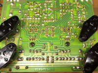
Attachments

- Home
- Amplifiers
- Solid State
- Accuphase E-303 DC-offset issue