I recently assembled this amp and it is running good.
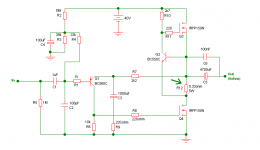
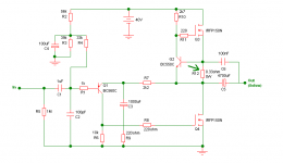
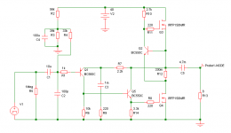
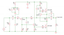
For the place of the CCS load resistor (R12) I have tried both the configs shown in the two pictures and both simulate and work fine with the distortion figures being identical at 1kHz@10V P-P into 8ohm.
My questions are:-
What are the advantages/disadvantages of the two CCS configs?
How can I reduce THD without adding more gain stages?
Thanks.
.
Attachments
Hi shaan, i can't help you with the CCs
I have a possible suggestion to get the THD lower though 😉 Try substituting R6 (10k) on the collector of the input transistor & put a simple constant current in it's place. This should increase open loop gain & thus with feedback lower the overall THD..
I reckon 😀
I have a possible suggestion to get the THD lower though 😉 Try substituting R6 (10k) on the collector of the input transistor & put a simple constant current in it's place. This should increase open loop gain & thus with feedback lower the overall THD..
I reckon 😀
Member
Joined 2009
Paid Member
I see Nelson Pass Zen in this - you could do worse than review those designs.
I don't like that you have the small output bypass capacitor on a different side of the resistor than the main output capacitor - easthetically speaking.
The first circuit is not a CCS, but closer to SRPP with Q2 monitoring current flow through R12 that is flowing through output device Q4 and therefore is modulated by the signal. Look at Zen version 4 for an example.
The second circuit is a CCS load since Q2 monitors current flowing through R12 which sees only the current through output device Q3. Look at Zen version 1 to learn about this one.
Why do you want to reduce THD further - these designs (Zen amps) are known to sound wonderful. It usually helps to push more current through the output devices but you already have 2 Amps bias current.
Member
Joined 2009
Paid Member
I nearly missed it - add a bootstrap capacitor from the output to the junctions of R10 and R11, this will provide a much better current supply for Q2. You might like to reduce R10 to around 1k.
Hi shaan, i can't help you with the CCs
I have a possible suggestion to get the THD lower though 😉 Try substituting R6 (10k) on the collector of the input transistor & put a simple constant current in it's place. This should increase open loop gain & thus with feedback lower the overall THD..
I reckon 😀
Thanks for the suggestion.
Are you sure about this? I'm only asking as the upper mosfet gate won't be driven linearly. It's gate voltage is controlled by the transistor that's effectively turning it into a constant current. Bootstrap to that & the CC is no longer a CC but a very modulated one.I nearly missed it - add a bootstrap capacitor from the output to the junctions of R10 and R11, this will provide a much better current supply for Q2. You might like to reduce R10 to around 1k.
You did give me a good idea on how to make the amp swing right to the positive rail though (or damn near). Split R10 into two resistors & then use a bootstrap from the output & connect it to the junction of the two new resistors replacing R10. If you don't do this you'll not get enough gate voltage on the upper mosfet to get right close to the rail.
You could try something else to lower THD as well. Whether you adopt a constant current instead of R6 on the collector of the input transistor or not, there would be a distinct advantage to placing a simple emitter follower where the lower power mosfet is connected.
Right now the input transistor is dealing with the current accross R6 & the current needed to charge the gate of the mosfet. If you can get rid of the gate charging from the input transistor (whilst increasing the current available to charge the gate) the whole thing will speed up & again you should see a lowering of THD.
It's a nice simple circuit, thought about the same sort of thing quite often. Seeing this makes me want to experiment 😀
Have fun 😉
Your output looks like this one:
http://www.diyaudio.com/forums/pass-labs/37038-excellent-srpp-power-amp-mosfet-4.html#post1982249
http://www.diyaudio.com/forums/pass-labs/37038-excellent-srpp-power-amp-mosfet-4.html#post1982249
Member
Joined 2009
Paid Member
Are you sure about this? I'm only asking as the upper mosfet gate won't be driven linearly. It's gate voltage is controlled by the transistor that's effectively turning it into a constant current. Bootstrap to that & the CC is no longer a CC but a very modulated one.
You did give me a good idea on how to make the amp swing right to the positive rail though (or damn near). Split R10 into two resistors & then use a bootstrap from the output & connect it to the junction of the two new resistors replacing R10. If you don't do this you'll not get enough gate voltage on the upper mosfet to get right close to the rail.
Yes, that's what I was thinking of, thanks for correcting me 😎
You could try something else to lower THD as well. Whether you adopt a constant current instead of R6 on the collector of the input transistor or not, there would be a distinct advantage to placing a simple emitter follower where the lower power mosfet is connected.
Right now the input transistor is dealing with the current accross R6 & the current needed to charge the gate of the mosfet. If you can get rid of the gate charging from the input transistor (whilst increasing the current available to charge the gate) the whole thing will speed up & again you should see a lowering of THD.
It's a nice simple circuit, thought about the same sort of thing quite often. Seeing this makes me want to experiment 😀
Have fun 😉
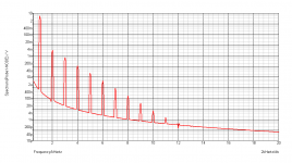
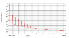
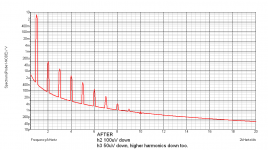
I'm having fun for sure. Your suggested additions showed very good improvements of the THD figures. Sim result below. I am going to try this tonight. 😀
Please tell me on the value of the emitter resistor for Q5.
Thanks.
.
Attachments
You did give me a good idea on how to make the amp swing right to the positive rail though (or damn near). Split R10 into two resistors & then use a bootstrap from the output & connect it to the junction of the two new resistors replacing R10. If you don't do this you'll not get enough gate voltage on the upper mosfet to get right close to the rail.
Bootstrapping is a good idea too.
Cheers for understanding, i'm not here to upset people 🙂Yes, that's what I was thinking of, thanks for correcting me 😎
It needs to be fairly low, i'd suggest 680R, don't forget that this is the only thing that will be discharging the gate. By the way, don't connect the emitter follower collector to the output or you'll restrict the voltage swing of the amplifier. Don't forget that to get near to the negative rail the mosfet will need up to 6V or more to get close 😉 Connect the collector to the positive rail. If you find dissipation an issue i'd suggest something like a zener diode in between the collector & the +ve rail to lower dissipation of the transistor. Noise shouldn't be an issue as it'll be on the collector 😀I'm having fun for sure. Your suggested additions showed very good improvements of the THD figures. Sim result below. I am going to try this tonight. 😀
Please tell me on the value of the emitter resistor for Q5.
E2A:- You could make a 12V rail from the ground of the amplifier. Again a simple zener & capacitor fed by a resistor from the positive rail. Not much current will be consumed as it'll only be used to charge the mosfet gate & this will increase at high frequencies. It still won't be a lot though... Food for thought.
I think i'm going to make something like this to drive a pair of Celestion Ditton 66 Monitors that i have in another room. It just needs to be done, i love the simplicity 😉
Last edited:
Hi Shaan
I'm surprised they measure the same.
In your second pic (with R12 above), R12 and Q2 measure the current through Q3 and try to keep it constant, so Q2 and Q3 form a constant current source and Q4 delivers the signal current to the load.
The circuit in the first pic (with R12 below) works differently, though. Now R12 and Q2 measure the current through Q4. Q2 tries to keep the current through Q4 constant by changing the current through Q3. So Q3 ends up delivering most of the signal current to the load, with Q4 only contributing a little.
If you split R12, half above and half below, you can turn it into a push-pull amp, where Q3 and Q4 each deliver about half the signal current to the load. That way you should be able to get about double the peak output current for the same idling current.
I'm not 100% sure of all that, but the sim should be able to tell you what currents are flowing in Q3 and Q4 for each configuration.
Also - if you bootstrap R10, you should be able to get more voltage swing on the output.
It's probably worth having a look at overload behavior as well - voltage clipping with a high impedance load and also current limiting with a low impedance load.
For distortion, you could try reduce R7 and R9 by half and see what happens. Maybe you could try reducing R6 by half as well. I don't know what that will do to the overall distortion, but it should improve the speed and maybe give better performance at high frequencies.
😕
Cheers - Godfrey
Edit: Oops, This is a bit late - I missed all of the other replies.
Last edited:
a bit
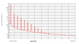
Quick sims show some more improvement of the harmonic content with Q5 collector at +ve and 1k emitter load. 2nd and 3rd harmonic about 100uV lower and higher harmonics are a bit lower too.
Cheers for understanding, i'm not here to upset people 🙂
It needs to be fairly low, i'd suggest 680R, don't forget that this is the only thing that will be discharging the gate. By the way, don't connect the emitter follower collector to the output or you'll restrict the voltage swing of the amplifier. Don't forget that to get near to the negative rail the mosfet will need up to 6V or more to get close 😉 Connect the collector to the positive rail. If you find dissipation an issue i'd suggest something like a zener diode in between the collector & the +ve rail to lower dissipation of the transistor. Noise shouldn't be an issue as it'll be on the collector 😀
E2A:- You could make a 12V rail from the ground of the amplifier. Again a simple zener & capacitor fed by a resistor from the positive rail. Not much current will be consumed as it'll only be used to charge the mosfet gate & this will increase at high frequencies. It still won't be a lot though... Food for thought.
I think i'm going to make something like this to drive a pair of Celestion Ditton 66 Monitors that i have in another room. It just needs to be done, i love the simplicity 😉
Quick sims show some more improvement of the harmonic content with Q5 collector at +ve and 1k emitter load. 2nd and 3rd harmonic about 100uV lower and higher harmonics are a bit lower too.
Attachments
Hi Shaan
I'm surprised they measure the same.
In your second pic (with R12 above), R12 and Q2 measure the current through Q3 and try to keep it constant, so Q2 and Q3 form a constant current source and Q4 delivers the signal current to the load.
The circuit in the first pic (with R12 below) works differently, though. Now R12 and Q2 measure the current through Q4. Q2 tries to keep the current through Q4 constant by changing the current through Q3. So Q3 ends up delivering most of the signal current to the load, with Q4 only contributing a little.
If you split R12, half above and half below, you can turn it into a push-pull amp, where Q3 and Q4 each deliver about half the signal current to the load. That way you should be able to get about double the peak output current for the same idling current.
I'm not 100% sure of all that, but the sim should be able to tell you what currents are flowing in Q3 and Q4 for each configuration.
Also - if you bootstrap R10, you should be able to get more voltage swing on the output.
It's probably worth having a look at overload behavior as well - voltage clipping with a high impedance load and also current limiting with a low impedance load.
For distortion, you could try reduce R7 and R9 by half and see what happens. Maybe you could try reducing R6 by half as well. I don't know what that will do to the overall distortion, but it should improve the speed and maybe give better performance at high frequencies.
😕
Cheers - Godfrey
Edit: Oops, This is a bit late - I missed all of the other replies.
Thanks for info on the CCS.
I don't want to run it as a push-pull. 10 watts will be enough for me with this circuit. thanks for the suggestion though.
I think I will use the bootstrap for better +ve swing.
I think i'm going to make something like this to drive a pair of Celestion Ditton 66 Monitors that i have in another room. It just needs to be done, i love the simplicity 😉
Please share the details when you do.
Thanks.
.
I should imagine that's simply down to the lower resistance value.Quick sims show some more improvement of the harmonic content with Q5 collector at +ve and 1k emitter load. 2nd and 3rd harmonic about 100uV lower and higher harmonics are a bit lower too.
Now try replacing R6 with a simple constant current. An NPN transistor, two diodes & a resistor will give you a good idea to see if it's worth persuing. again connect from the base of the transistor to the +ve rail. I'd suggest a resistor of about 270R to set the CC. This will result in about 2.7mA continuous through the input transistor collector.
It should speed things up & result in lower distortion yet again.
I wish i could sim things this quickly lol 🙂
Of course 🙂 I think you'll see something else before that though, i'm just gathering stuff together (including test gear) for a new project that will be turned into a thread on here when i get it all together.Please share the details when you do.
Thanks.
Bests, Mark.
Last edited:
- Status
- Not open for further replies.
- Home
- Amplifiers
- Solid State
- About This "Simple Machine"