Hi,
I drew up this PS design and wonder if it looks ok. Everything on the design is stolen from somone. Thanks, Nelson (TOAO), Syl and others not named.
I am concerned with a few things:
Are all of those film caps on the electrolytics a waste?
Is the RC filter for the front end properly drawn?
How do I calculate the R and the C for that filter?
Is there a better design for the bridge diode snubbers?
Is the grounding scheme the right way to go?
The Schematic follows.
Thanks
Attachments
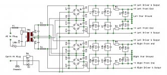
I think Bridge B2 and B4 should be mirrored left to right
also B4 lacks one DC output
For the R in RC, you need to know how much voltage drop
you can accept. This drop depends on the current consumption.
After that you select the caps to acheive
the filter roll off frequency.
This frequency should of cause be somewhere below 100 Hz
to block hum from trafo, more or less.
A bridge rectifier produces 2x50Hz signals.
This cut off (f) can be as low as 1 Hz, with big Caps
RC=1/(2pi x f)
C=1/(2pi x f x R)
f=1/(2pi x RC)
Ooops
Saw something myself!
The output from B3 Should read "+V Right Driver & Output"
And
F2 and F3 might be replaced with four fuses on the other side of the node to the right. That is, one fuse for + and - for each channel.
Thoughts?
Thanks,
ab
Saw something myself!
The output from B3 Should read "+V Right Driver & Output"
And
F2 and F3 might be replaced with four fuses on the other side of the node to the right. That is, one fuse for + and - for each channel.
Thoughts?
Thanks,
ab
halojoy said:This frequency should of cause be somewhere below 100 Hz
to block hum from trafo, more or less.
A bridge rectifier produces 2x50Hz signals.
This cut off (f) can be as low as 1 Hz, with big Caps
In the USA, the frequency of concern will be 120Hz.
- Status
- Not open for further replies.