Mooly,
That's my fault for giving you incomplete information on my setup and for me not understanding what I was looking at. There certainly is a lot going on, and without your guy's help I never would have made it this far.
I am currently just using a potentiometer as shown in your schematic. I have everything on a breadboard for the moment, so I could switch to a Vbe multiplier arrangement as you describe without too much difficulty. This follows a similar line of thought as my idea to add a diode in series with the potentiometer in the current arrangement. I will try to reupload my current schematic at some point today if I can.
Yes, for sure - without the thermal feedback, the output stage quiescent current will never be stable and the runaway will always be a danger, so... go for the spreader 😉
You can use one of your small 2N2904's, gluing it to the output heatsink, or - even more convenient - some TO-126 device, like BD139 or MJE340 - it's easy to screw it on top of one of your output transistors.
You can use one of your small 2N2904's, gluing it to the output heatsink, or - even more convenient - some TO-126 device, like BD139 or MJE340 - it's easy to screw it on top of one of your output transistors.
Mooly,
That's my fault for giving you incomplete information on my setup and for me not understanding what I was looking at.
🙂 Not at all. I remember my first attempts at designing and building and circuits in the days before the internet... its all hard won knowledge at the end of the day. You only really learn by doing and making mistakes and seeing how things interact when they all come together.
Just using a pot for bias will be very unstable. The best you can hope for is that by setting the bias really low (the 10ma I mentioned) it shouldn't go destructively high as the amp warms. If you have 10ma cold and 150ma hot then its lousy from a stability point of view, but you get a 'working' amp that you can listen to for a while. And that's important. To hear it working. As far as distortion goes, even a bias current of a milliamp or two is enough to reduce most of it.
All,
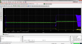
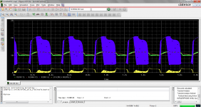
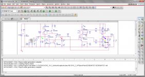
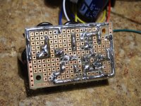
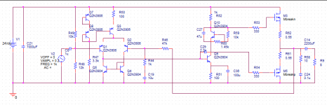
Attached is my current schematic. Also, I have attached plots of the "motorboating" that I was able to replicate in my simulation when I added a 2 Ohm resistor in series with my power rail (for C21=470uF, C21=10uF, and C21=10uF and C19=9000uF, respectively). To stop this, I have changed C21 to 9000uF and C19 to 10uF and also made the same changes to the physical hardware. R56 is the trimmer I am using to set the bias current. If I understand correctly, replacing R56 with a transistor and using a trimmer to bias it should be sufficient to provide thermal compensation? (see schematic w/ proposed change)
Attached is my current schematic. Also, I have attached plots of the "motorboating" that I was able to replicate in my simulation when I added a 2 Ohm resistor in series with my power rail (for C21=470uF, C21=10uF, and C21=10uF and C19=9000uF, respectively). To stop this, I have changed C21 to 9000uF and C19 to 10uF and also made the same changes to the physical hardware. R56 is the trimmer I am using to set the bias current. If I understand correctly, replacing R56 with a transistor and using a trimmer to bias it should be sufficient to provide thermal compensation? (see schematic w/ proposed change)
Attachments


The transistor bias should be a huge improvement but it needs the transistor to be in contact with the heatsink. Adding the low value source resistors we mentioned earlier would also help.
All,
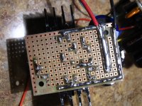
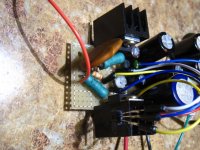
I made what I think may be the final round of modifications to the circuit (maybe?). I tested everything and soldered it to a new circuit board. My changes include adding a "spreader" biasing transistor (Q10) as per everyone's suggestions, adding two 0.56 Ohm source resistors, changing C29 to 2.2nF (there seemed to be some residual high frequency noise, hopefully that change won't be an issue), and changing R48 to 12k to better center the bias point.
In addition, to avoid any power supply resistance issues moving forward, I soldered on some slightly beefier power supply cables. In order to mount the biasing transistor on the heatsink, I stuck it to the side of the heatsink of the IRF540N with a bit of heatsink grease and some super glue. A bit crude, perhaps, but the bias current seems to be considerably more stable now.
Unless folks have any additional suggestions for this design, I may call it here on this project. Honestly, I'm pretty surprised that I was able to debug this design so quickly and effectively, and a big thanks to everyone for their guidance on this. In particular, I think that gaining a better understanding of gain and phase characteristics will give me a better handle on designing and debugging heavily feedback-controlled designs like this, which are still fairly new territory for me. My eventual plans are to start moving towards higher power in my designs, as well as some possible experimentation with class D designs...
Attachments
I think as you suggest that you have probably gone about as far as you can with this build. The only thing you could add as a trial would be a series input resistor and a small cap across R48.
Have you listened to it yet ?
Have you listened to it yet ?
Good job 🙂
The only simple thing, I would add for lower distortion (and improved sound quality) - bootstrapped VAS load (dynamic load).
For that purpose, you have to replace R52 (1k) with a series of 2 resistors, say, 470R each, and add a 100uF electrolytic between that middle point and the output (+ to the resistors). This way, you will significantly increase the dynamic impedance of the VAS load 😎
Cheers,
Valery
I think as you suggest that you have probably gone about as far as you can with this build. The only thing you could add as a trial would be a series input resistor and a small cap across R48.
Have you listened to it yet ?
Both of those should be fairly doable. I presume your original prescription of 220-1k on the input resistor should still be the same? what would you recommend on the cap, maybe 1 nF, or perhaps less?
I have listened to it just a little bit on some music, and I would say it sounds pretty good. I can't say that I have really developed much of an ear for this yet, though, so this design will probably serve as my yardstick for judging future builds.
The only simple thing, I would add for lower distortion (and improved sound quality) - bootstrapped VAS load (dynamic load).
Thanks. I'll look into that, hopefully that shouldn't be too hard to do. Unfortunately, my insistence on tight layouts on tiny boards makes re-soldering components a real pain. 😀
Yes, something like 1k and 1nf should be easy to implement as a test.
This is an old thread but it gives an idea of what happens as layout is changed. The amp here is far more 'forgiving' of wiring errors because it doesn't use a differential input stage.
http://www.diyaudio.com/forums/solid-state/126370-oscillograms-testing-why-layout-matters.html
This is an old thread but it gives an idea of what happens as layout is changed. The amp here is far more 'forgiving' of wiring errors because it doesn't use a differential input stage.
http://www.diyaudio.com/forums/solid-state/126370-oscillograms-testing-why-layout-matters.html
@ Jiny,
See post #48. You need a dynamic load on your voltage gain stage to replace R52. That will give you more feedback to work with. In using a 1k resistor for your collector load you are limiting this while expecting a closed loop gain of 48.
Further the 1k provides a low impedance path for spurious switching elements from the output stage impressed on the supply rail common to your voltage amplifier stage. As far as the latter is concerned these need to be suppressed - not recycled.
Further the 1k provides a low impedance path for spurious switching elements from the output stage impressed on the supply rail common to your voltage amplifier stage. As far as the latter is concerned these need to be suppressed - not recycled.
Exactly - that's the other advantage of dynamic load.
Staying close to 1k in static, it becomes a much higher value in dynamic - that's what you'd like it to be.
All,
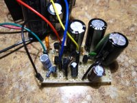
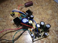
I have made the final few tweaks as per everyone's recommendations (see updated schematic). I have split R52 into two 510 Ohm resistors and added the bootstrapped VAS load, I have also added in a 1nF capacitor at the input (see C38) and a 1K resistor in series with the input capacitor (see R64).
Mooly, just out of curiosity, what is the exact function of the 1k input resistor R64? I have tried it both ways side by side as a test, and I can't seem to tell any difference with or without it. is it just there as a safety measure against high frequency noise or to mitigate reactive input loading from C38 perhaps? I would like to better understand what this is for in terms of my future designs.
Attachments
All,
I have made the final few tweaks as per everyone's recommendations (see updated schematic). I have split R52 into two 510 Ohm resistors and added the bootstrapped VAS load, I have also added in a 1nF capacitor at the input (see C38) and a 1K resistor in series with the input capacitor (see R64).
Mooly, just out of curiosity, what is the exact function of the 1k input resistor R64? I have tried it both ways side by side as a test, and I can't seem to tell any difference with or without it. is it just there as a safety measure against high frequency noise or to mitigate reactive input loading from C38 perhaps? I would like to better understand what this is for in terms of my future designs.
OK. Cool 😎
R64 and C38 form an input low pass filter (1-st order), preventing unwanted HF signals from entering and being amplified by the amp.
The cut-uff frequency is calculated as F = 1 / (2 * Pi * R * C), giving 159KHz in your case, which is fine.
Making it too low will limit the rise/fall time (rounded corners on the square wave response), making it too high will just let the HF passing through the amp. In the modern high-speed amps some 300KHz is a good compromise.
Cheers,
Valery
Mooly, just out of curiosity, what is the exact function of the 1k input resistor R64? I have tried it both ways side by side as a test, and I can't seem to tell any difference with or without it.
Its as vzaichenko says, its a simple first order R/C filter to protect the amp from any unwanted hf from entering. Its fairly standard practice to have something like this on an amplifier input.
It could also alter (help or otherwise) a design of marginal stability due to layout and grounding compromises.
Ok, that's what I figured. Just wanted to be sure.
Also, Mooly, that thread about layout was a fun read. I have some background in amateur radio, so I am definitely familiar with the consequences of ground loops. Also, Seeing that one technique for working with SOT and SOIC packages on perf board in a sort of vertical card arrangement was pretty impressive. 😱
Even when working on breadboards, I definitely try to avoid having overly long signal or ground paths. In future designs, I will probably not want to split my layout across two boards the way I have on this build, but I have a whole pack of those small perf boards that I need to use up at some point, and at a mere 5 Watts RMS, I won't exactly be blowing out any speakers with this amp 🙄. My resistance issue with my power leads was a new one for me, as I have never really worked at significant enough power that it would matter as long as my decoupling caps were high enough. something to remember for next time, I suppose.
As stated, I think I am happy with where I ended up with this design, so I am ready to call things here. It has been a pleasure working with you all, and with any luck you may be hearing from me again soon-- hopefully to talk about my successful builds instead of trying to debug them! 😱
Until next time,
JLNY
Pleased you enjoyed it 🙂 and you've done really well actually in taking a design of your own and seeing it through to a finishing point.
You can do a lot with 5 wrms. Give this a try sometime,
http://www.diyaudio.com/forums/mult...much-voltage-power-do-your-speakers-need.html
There are many designs and approaches you could try, and I would recommend something using a 'single ended' input rather than a complex differential stage. These tend to be far more forgiving of layout problems and as bonus 🙂 can sound absolutely superb.
You know where we are anyway...
- Status
- Not open for further replies.
- Home
- Amplifiers
- Solid State
- AB amplifier is oscillating. seeking critique