There are a few traders now advertising cheap PCBs.
Be very wary, I purchased two of these produced using a home CNC router. On the surface it looks OK and all the tracks are insulated from each other and the holes all line up and are the correct size.
PROBLEM, the CNC process almost invariably leaves behind a lot of surplus copper.
This was just a simple DATA amplifier. On the breadboard the design works flawlessly and the correct PCB works perfectly too.
This cheaply produced PCB made a perfect HF oscillator. The capacitance of the spare copper obviously made some pretty nice capacitors which ruined the overall design.
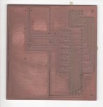
Attachments
I wouldn't necessarily call it cheaply produced (you're not complaining about shorted or broken traces), but rather, cheaply "designed." The problem appears to be not just the surplus copper, but what circuit nodes they're connected to. If "senstitive" nodes could be identified (by the person who designed the circuit or who is knowledgeable about it), the routing software could perhaps be modified to cut off the excess copper of such nodes, and add holes for jumper connections between the excess copper and nearby grounds. This would make it more like a conventional board with ground fill. Can you ask the maker if there's a way to specify this? If they respond that "it's electrically correct" then you know not to use them again...
This problem is similar to a pcb layout person or autorouting software making a board form a switching regulator schematic with no knowledge of where the high-speed/high current loops are and what to do with them, or really any knowledge of electronics.
This problem is similar to a pcb layout person or autorouting software making a board form a switching regulator schematic with no knowledge of where the high-speed/high current loops are and what to do with them, or really any knowledge of electronics.
The CNC routing process does not leave excess copper if the tools are in good condition (solid carbide only!) abd the machine is properly set up. We use LPKF CNC routers for prototype production at work all the time, and the output is pretty satisfactory, only sometimes requiring cleanup.
The excess copper here is the large copper areas, nothing to do with the cutter condition. Theses are unavoidable in the way these cutters do a generic PCB, they work by cutting a path of the clearance round any signals, so simplifying the CNC router path and minimising the time taken to produce a PCB. To clear polygon areas involve much more post processing, then machining time increases as does tool wear. So either tie the copper to the GND/0V signal for digital boards or get etched PCBs where these areas of copper are not desired.
hmm, I was thinking of doing something similar, but less complex (and by hand not cnc). Top layer will be a ground plain. I think tying big unused area's on the bottom side to grond sounds like a plan 🙂
Tony.
Tony.
I made a crude PCB for a crossover by gouging out copper (ISTR with a Dremel cutoff wheel) on a blank copper-clad board for a speaker crossover. It was interesting doing a "layout" by cutting the copper into large rectangles. Sorry, don't have a pic, and don't know where it went.
Tin plated PCBs | Learn to Solder
Crass announcement, the (third annual) Atlanta Mini Maker Faire is THIS Saturday on the Georgia Tech campus. Hmm, no self-made audio equipment there as far as I know ... I may have to change that for next year. If only I had thought of it, we could have a few of us there for an East Coast version of Burning Amp. Again, maybe next year.
Here's a small board (an AA-cell powered LED flasher) made for the learn-to-solder table at the Atlanta Mini Maker Faire last year - they were made on a small CNC machine:hmm, I was thinking of doing something similar, but less complex (and by hand not cnc). Top layer will be a ground plain. I think tying big unused area's on the bottom side to ground sounds like a plan 🙂
Tony.
Tin plated PCBs | Learn to Solder
Crass announcement, the (third annual) Atlanta Mini Maker Faire is THIS Saturday on the Georgia Tech campus. Hmm, no self-made audio equipment there as far as I know ... I may have to change that for next year. If only I had thought of it, we could have a few of us there for an East Coast version of Burning Amp. Again, maybe next year.
The CNC routing process does not leave excess copper if the tools are in good condition (solid carbide only!) abd the machine is properly set up. We use LPKF CNC routers for prototype production at work all the time, and the output is pretty satisfactory, only sometimes requiring cleanup.
This is an LPKF board and they can be made so that this doesn't happen. Having spent many hours with the system I would not let something like this go out. Tool sharpness and tool height alone can fix this problem. Looks like someone needs to spend more time with the machine. You can also specify that any area of copper be removed so I would create a wider "isolation" around tracks. This is a function of the LPKF processing software and again someone doesn't know how to set that up or doesn't care.
It may have been a crude CNC setup rather than an LPKF or similar. We use a pair of LPKF machines at my work place for prototyping. Even they have problems if the tools are not adjusted properly and replaced periodically. Having said that, I wouldn't send out a board like that, either.
- Status
- Not open for further replies.
- Home
- Design & Build
- Parts
- A warning about cheap PCBs