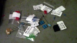
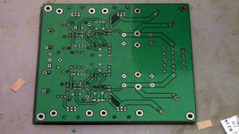
I am finally getting my Buffalo III build on the way. The mid-range hash I hear in my present DAC has finally got to me, so it is time.
I bought the older, multi-channel version of the Buffalo III, from a fellow diyAudio member in Swap Meet in 2014. At some point, I will need to double check that I have the right firmware with the DAC module, as this kit has been waiting to be built for a long time. I think the former owner had it awhile also.
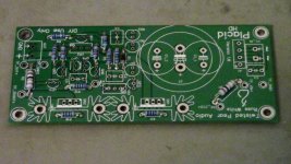
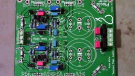
This kit contains the original Placid HD supplies: v-1.0.
At this point in time, I am building a standard stereo build, although I may explore redoing this module as a four channel version, if I decide this is the right DAC for my system. In any case, I will eventually have a multi-channel DAC of some kind, be it several modules of Buffalo or something else.
I am not an authority on electrical engineering by any means. My true joy is learning and creating things. My education is in Fine Arts, so what I am offering here is a Buffalo building journey from a non expert point of view. I enjoy speaker building the most, but dabble in electrical kits to get the best from my creations. To date, I have completed a Peter Daniels LM3875 kit, a LightSpeed volume control, a First One v1.4 kit, and am half way thru an off the wall tube pre-amp build. So that would make the Buffalo III my first "intense" circuit board soldering project. Most of my soldering experience is in Stained Glass Art. 🙂
So at the very least, I am hoping my journey will help someone else who is maybe on the fence on whether or not they want to venture this project themselves.
The literature the designers provide is pretty good, esp, if You have a solid understanding of electrical components and circuits. I do not work in that realm everyday, so I will be double checking some things as we proceed.
So lets get started...😀
I bought the older, multi-channel version of the Buffalo III, from a fellow diyAudio member in Swap Meet in 2014. At some point, I will need to double check that I have the right firmware with the DAC module, as this kit has been waiting to be built for a long time. I think the former owner had it awhile also.
This kit contains the original Placid HD supplies: v-1.0.
At this point in time, I am building a standard stereo build, although I may explore redoing this module as a four channel version, if I decide this is the right DAC for my system. In any case, I will eventually have a multi-channel DAC of some kind, be it several modules of Buffalo or something else.
I am not an authority on electrical engineering by any means. My true joy is learning and creating things. My education is in Fine Arts, so what I am offering here is a Buffalo building journey from a non expert point of view. I enjoy speaker building the most, but dabble in electrical kits to get the best from my creations. To date, I have completed a Peter Daniels LM3875 kit, a LightSpeed volume control, a First One v1.4 kit, and am half way thru an off the wall tube pre-amp build. So that would make the Buffalo III my first "intense" circuit board soldering project. Most of my soldering experience is in Stained Glass Art. 🙂
So at the very least, I am hoping my journey will help someone else who is maybe on the fence on whether or not they want to venture this project themselves.
The literature the designers provide is pretty good, esp, if You have a solid understanding of electrical components and circuits. I do not work in that realm everyday, so I will be double checking some things as we proceed.
So lets get started...😀
Starting the Placid HD v 1.0
You know how these things go, You order this stuff, then You get it, get overwhelmed, and wonder what You get yourself into. 😱
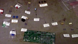
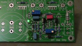
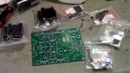
I decided to start simple, with the Placid HD:
I have the original version, so it is a little different then the new boards.
What I can say, Russ, Brain and Leon, have done a great job designing, packing and presenting these kits. All the parts are clearly labeled and the boards clearly marked. It reminds me of paint by numbers. Find the part, find the part number on the board and solder it in, and away we go.
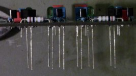
As suggested in the manual, I started with the resistors, as they are the lowest components. It took awhile to get the technique right to bend the wires on the resistors so they were "perfectly" centered in their "rectangles" on the board. Once bent, I would thread the resistors thru, dab on some flux (using a toothpick), solder, then clip the excess wires off.
You know how these things go, You order this stuff, then You get it, get overwhelmed, and wonder what You get yourself into. 😱
I decided to start simple, with the Placid HD:
I have the original version, so it is a little different then the new boards.
What I can say, Russ, Brain and Leon, have done a great job designing, packing and presenting these kits. All the parts are clearly labeled and the boards clearly marked. It reminds me of paint by numbers. Find the part, find the part number on the board and solder it in, and away we go.
As suggested in the manual, I started with the resistors, as they are the lowest components. It took awhile to get the technique right to bend the wires on the resistors so they were "perfectly" centered in their "rectangles" on the board. Once bent, I would thread the resistors thru, dab on some flux (using a toothpick), solder, then clip the excess wires off.
Attachments

polarity or not
Resistors are pretty straight forward, they can not be installed backwards. But I knew diodes had to go in one way. Thankfully, the board is marked with a band in the diode rectangle, echoing the band on the diode itself. It is so simple, one could miss it. I am farsighted, so I need to be even more observant, even with reading glasses.
Resistors are pretty straight forward, they can not be installed backwards. But I knew diodes had to go in one way. Thankfully, the board is marked with a band in the diode rectangle, echoing the band on the diode itself. It is so simple, one could miss it. I am farsighted, so I need to be even more observant, even with reading glasses.
Attachments
directions...
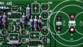
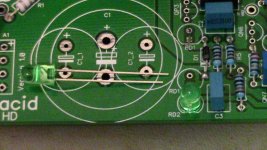
Next up were the small caps. These were not polarized.
But the variable resisters (VR) needed to go in a certain way to work right for adjustments. Once again, a close look at the board revealed the answer: There is a tiny circle symbol echoing the screw location in the VR rectangles.
The LEDs took me awhile to figure out. I soldered the first one backwards in fact. The board has a circle with a flat bottom to dictate polarity, the flat part being the negative side. I could not see the flat part in the LED itself, it was pretty subtle. A google search reminded me, that the long wire is the positive side, so I want with that. Thankfully, I do not think the newer boards have the LEDs. 😉
After that, he Rectifier seemed pretty easy, with the big "plus" sign stamped on the side...
Attachments
Almost done apart from thermo coupling...
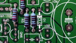
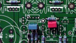
Likewise, the big cap was clearly marked, with the minus symbol banded down one side...
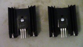
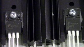
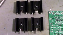
After that, I thermo pasted the regulators to their heatsinks. I felt right at home soldering the heatsinks to the board, that is more of the size of solder bead I am used to doing, when assembling glass work. 😉
I used alcohol to clean the flux off the board. I used both a cotton rag and a tooth brush to get it all. It is pretty tricky, due to the "catchy" nature of the solder beads and clipped wires. Patience is a virtue here.
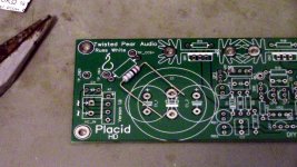
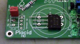
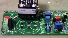
The Placid is almost done, it is missing one thing:
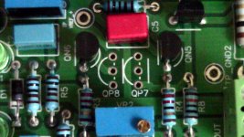
Based on the instructions, transistors QP 7 and QP 8 need to be "thermo coupled". There was a picture of that, but I could not tell what was really going on.
Are the transistors just physically touching? Or are they thermo pasted together and wrapped around with tape? Or are they bonded together (not needing thermo paste)?
Once I know what proper "thermo coupling" is, I will install the transistor pair in, and have the DAC Placid done. 🙂
Next weekend, I can start the Placid HD Bipolar, which should go really well, as it is two more of these boards.
I hope the photos help
Allen
Likewise, the big cap was clearly marked, with the minus symbol banded down one side...
After that, I thermo pasted the regulators to their heatsinks. I felt right at home soldering the heatsinks to the board, that is more of the size of solder bead I am used to doing, when assembling glass work. 😉
I used alcohol to clean the flux off the board. I used both a cotton rag and a tooth brush to get it all. It is pretty tricky, due to the "catchy" nature of the solder beads and clipped wires. Patience is a virtue here.
The Placid is almost done, it is missing one thing:
Based on the instructions, transistors QP 7 and QP 8 need to be "thermo coupled". There was a picture of that, but I could not tell what was really going on.
Are the transistors just physically touching? Or are they thermo pasted together and wrapped around with tape? Or are they bonded together (not needing thermo paste)?
Once I know what proper "thermo coupling" is, I will install the transistor pair in, and have the DAC Placid done. 🙂
Next weekend, I can start the Placid HD Bipolar, which should go really well, as it is two more of these boards.
I hope the photos help
Allen
Attachments


The Placid is almost done, it is missing one thing:
Based on the instructions, transistors QP 7 and QP 8 need to be "thermo coupled". There was a picture of that, but I could not tell what was really going on.
Allen
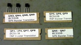
QP7 and QP8 are both facing "same way", flat side of the transistor points the same way. This way it's not quite possible to do a good thermo coupling.
Don't bother, it will do just fine without thermo coupling. Just bring the two transistors close to each other - or do as I did, mount them nicely and forget about the thermo aspect.
A closer look...
Thanks avr300, I am glad You caught that too! 😱
I took a closer look this morning, with a fresh eye, and realized they are indeed the same way. Getting version manuals mixed up. 😱
Glad I did not have these thermo coupled ahead of time. 😉
QP7 and QP8 are both facing "same way", flat side of the transistor points the same way. This way it's not quite possible to do a good thermo coupling.
Thanks avr300, I am glad You caught that too! 😱
I took a closer look this morning, with a fresh eye, and realized they are indeed the same way.
Getting version manuals mixed up. 😱Glad I did not have these thermo coupled ahead of time. 😉
Attachments
I hope this juorney has a happy ending...
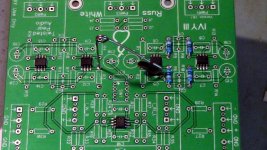
I got the Placid HD, Placid HD BP, IVY III and Buffalo III assembled and soldered.
I tested and calibrated the Placid's - no problem.
I measured the resistance on the outputs of IVY III with no power: SE outputs had 22.9 ohms between SE and GND and the balanced had 2.89 K ohms between GND and + and GND and -.
I powered up the IVY III, which was fine with the bulb tester but got smoke on Placid HD BP (by LED lights) at full power. With the bulb tester back on, I measured the IVY output resistance. The left SE output had around 22.6 ohms between GND and SE, and the balanced had the same stable k Ohm reading between GND and + or GND and - respectively. But the right side had a fluctuating number on both outputs. I took a closer look at IVY III, and found some flux residue on topside of the board. Cleaned it all off, going in between resisters and Caps where I could with cotton rags wrapped in tooth picks and the such. Now I get the same 22.6 ohms on the Left side and 18 ohms stable on the Right side. All the balanced outputs measured stable and the same. Placid BP worked for quite awhile, with stable voltages of 14.98/-14.98 and CSS current of 200 (150 mA for IVY and 50 mA recommended extra shunt current) on each side. After awhile, the minus side went to an unstable - 3 volts with the bulb having a faint glow. The positive side is still stable at 14.98 volts. Current is still stable on both sides. LEDs are dimmer on minus side.
So I am guessing what ever smoked, died. My guess would be the diode, but not sure.
Also, I am wondering if the Right SE output is compromised in the IVY, being it reads less then the Left. (I will be using the SE outputs 😱 )
Something also happened with the Placid hooked up to the Buffalo. At first, all was fine, except no "mute" LED and the LEDs on the AVCC module did not lit up. After awhile, the rectifier started to smoke. On inspection, I noticed a cold solder joint on jumper J7, it caused a 47 K reading instead of 0 ohm for that jump. I had a really hard time soldering these, between far sighted vision, depth perception challenges being completely blind in my right eye, and lack of the perfect sized soldering tip. In fact, I found the cold solder using the zoom on my camera. I did test these after I initially soldered and cleaned them, they all read 0 ohms at that time. I can only speculate that the SMD part had better "air" contact and the solder had not oxidized at that time. After I fixed that, the "mute" LED came on and the AVCC module lit up. Again, this worked fine for awhile, then the bulb got brighter and the rectifier started to hiss. The voltage before the hissing read 4.92 with the bulb tester on and 5.25 at full-power. I had the current set to 490 (450mA for the DAC and 40 Shunt). Was going to raise this for the SPDIF board, but did not get that far.
So, I would guess that the rectifier needs to be replaced on that Placid. Maybe, I will try to measure the current on that - do not like the hissing.
Also, again, I am wondering if the Buffalo DAC board has been compromised.
It was a great day, finishing the boards and successfully testing the power supplies which where ran full power for three hours, no problems.
Then followed by a day ending with two broken PSU's and possibly compromised boards.
Feeling pretty discouraged:
Not sure if I should grind ahead - the SMD solderingi s definitely beyond my capacity and available tools. Yet, I am sure the fixes are not too bad, just do not know what other damage may have been caused.
I wonder if I ought to send this to someone who can fix the issues and measure the boards to make sure nothing else is compromised.
I would like to post the photos of my build, but I am not too enthusiastic about that at the moment.
Any suggestions and help is greatly appreciated.
Thanks in advance,
Allen
Last edited:
Lets rewind a bit...
Yikes, no responses, a little unsettling...
I do feel a little better today, but still not sure where I am at with this DAC build.
I will at least post the photos of the build so far, at the very least, maybe someone will learn what NOT to do...
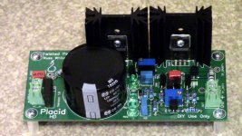
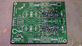
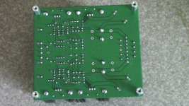
Here is the completed Placid HD.
Yikes, no responses, a little unsettling...
I do feel a little better today, but still not sure where I am at with this DAC build.
I will at least post the photos of the build so far, at the very least, maybe someone will learn what NOT to do...
Here is the completed Placid HD.
Attachments
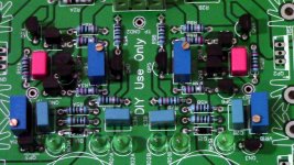
The Placid HD BP build: mounting transistors
The Placid BP is very similar to the regular Placid, just twice as many parts. Also, it is important to note, because the BP is a Bi-polar supply, it has a different transistor configuration on each side. As I mount the heatsinked transistors to their heatsinks first, before I solder, I relabeled the transistors to be sure I could identify them later...
The Placid BP is very similar to the regular Placid, just twice as many parts. Also, it is important to note, because the BP is a Bi-polar supply, it has a different transistor configuration on each side. As I mount the heatsinked transistors to their heatsinks first, before I solder, I relabeled the transistors to be sure I could identify them later...
Attachments
Placid BP resistors.
Like with the Placid, I started with the resistors. This was pretty straight forward, just more of them. After I cut all the leads off, I cleaned the board...
Like with the Placid, I started with the resistors. This was pretty straight forward, just more of them. After I cut all the leads off, I cleaned the board...
Attachments
Last edited:
Lower to higher
After building the regular Placid, I did realize that installing the small transistors after some of the taller Caps and Variable resistors, made it a little tricky to install the transistors. So this time around, I installed the short Caps first, followed by the small transistors, then the LEDs, followed by the higher Caps and Variable resistors. This had a much better flow to it, inregards to holding the parts in place while soldering.
I took special note of the Transistor types: NPN or PNP, as they are opposite on each side.
Also, all the LEDs are installed the same direction across the board.
With a symmetrical looking design like this, I had to be really mindful of when each side is a "mirror" of the other or an exact copy. The board and parts are very well labeled, just have to watch the mind tricks. 🙂
Attachments
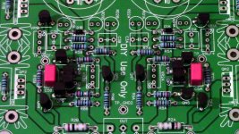
Now the big stuff
This was my favorite part, soldering the big stuff. Got the terminal blocks, big Caps, and heatsinked transistors in place and soldered.
Again, I had to make sure I had the right transistors in the right place, one side is NPN and the other PNP. The Caps, on the other hand were installed facing the same way. The polarities are clearly marked on the board.
I cleaned this again with alcohol and installed the standoffs.
Attachments
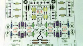
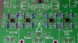
IVY III: kit and templates
IVY III is not really hard to assemble, but there are a lot of different resistors, so keeping track of these is the main thing. In the manual, there is a nice color coded guide to help give a visual layout of the different resistor positions.
As there where so many resistors, I created a little bending guide, so I could get the resistors better centered.
Attachments

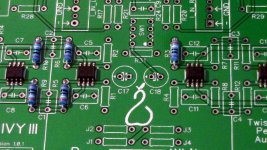
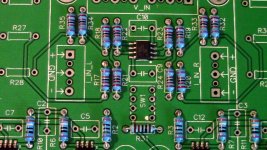
Lots of resistors
Even with the visuals, at first, when the board is blank, it is easy to solder a resistor in the wrong place (1st photo). My mind can play tricks with systematical patterns like this...
After un-soldering the resistor, the hole was filled with solder. As I do not have any wick, I heat the solder up and push it thru with a large safety pin. The solder does not adhere to the pin, so this works well. Also, the pin does not go completely thru the hole, so it does not poke my fingers either. 🙂
As the board gets populated, it gets easier to place the resistors in the right spot.
Also, this time around, I wanted to arrange the bands on the resistors into a symmetrical pattern. It is almost perfect, except for two pair on each side. 😱 Can You see which pairs? No biggie, as the pattern is still symmetrical anyway...
Attachments
Last edited:
Sorry you had trouble with the Placid. Version 1 has design defect. You should throw it out and either buy latest version or use another design dual supply.
My first placid BP v1 failed completely, made a weird noise every couple seconds. Some kind of oscillation my tech couldn't figure it out.
I had another v1 kit on hand so I just chucked the old one and built a new one. It lasted a few months, then it's voltage was all over the place. I kept a voltmeter connected to it all the time, I checked it every couple hours, it would change sometimes dramatically every hour.
I searched for solutions, finally found some reference to design issue on their own forum. I made my own simple dual supply with Belleson regulators.
A couple years ago I built a Buffalo2 for a friend using newest Legato and newest Placid, it works very well and is stable.
Good luck
Rich
- Status
- Not open for further replies.
- Home
- More Vendors...
- Twisted Pear
- A Visual Buffalo III Building Journey...