I want to offer you such an amplifier As a good replacement for the 3886 and 7293 microchips, which have become much more expensive. instead of 240/9240, you can use a very cheap 510/9510. In a differential cascade with a different correction, bipolar transistors can also be used, as cheaper and more accessible. In general, the spice model is below, pdf with a diagram and a *.Ley for ordering or reworking for yourself.
PS ^ I really want to know your opinion, it is dear to me.
PS ^ I really want to know your opinion, it is dear to me.
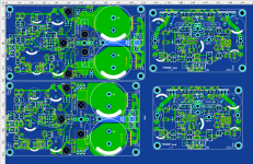
Attachments

No takers? Well, looks pretty standard fair stuff. Some petty comments might be:
1. I'm not sure high voltage 2n5401 are the best choice for the current mirror, possible poor early effect at real low voltage.
2. and 470 Ohm degen resistors on the current mirror is more than I would use but I guess it's OK, with only 1.25V on Q8, given R10.
3. but I'm not sure R10 is useful otherwise? R10 causes a bit of phase inversion on the positive clipping.
4. I'm curious how and why you used C3 + R22, and C11 and C13.
5. Is 20dB (10:1) enough gain? I would expect another 6dB or 10dB for a power amp of any size.
6. Did you use the phase margin simulation successfully? I deleted it to clean up the simulation.
7. I had to use a 2SK170 model that I had and may be different, so maybe you could post yours or add it to the schematic.
8. Both IPS do not have a lot of margins on breakdown voltage, so you might consider cascoding the IPS.
9. There is no decoupling on the IPS power supply. This will not show in simulations unless you add noise to the supply voltages.
10. Likewise, decoupling the VAS power supply will avoid half cycle current draw by the output causing distortion feedback to the VAS. Again, that will not show in simulations. Bruno has a paper about supply noise as it relates to the compensation that returns to the rail.
11. You've got 8 Volts between gates, as is typical. But this subtracts from the output swing. It is not difficult to ~bootstrap the gates to gain another 8VPP, which translates to about 100Watts vs 75Watts into 4 Ohms. You could also use a higher VAS voltage, ie +/-35V to +/-40V but not so much to cause rail sticking.
12. Perhaps the FETs are tough enough that output protection is not required??
13. But a output build-out inductor + resistor would prevent any loading from causing feedback instability.
14. and C5 should probably have a small resistor (~100) to limit RF current getting from the speaker line to the IPS, and picking up the local radio station.
15. Sometimes it's a good idea to put diodes on C2 to prevent the possibility of -30V getting to the gate/base of J2, causing latch-up.
Pick, pick, enough picky stuff. I'm sure others will have other issues. Enjoy your work. Looks like you have the basics down.
1. because I wanted more common transistors than even bc550/560
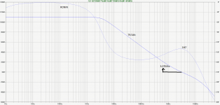
4. C3 + R22, and C11 and C13 were selected focusing on the stock by phase. I will attach a screenshot below
5. probably it was possible to add...
8. the supply voltage of 30v is taken as the most common in microchip amplifiers, even with a small margin
14. I have seen many without an additional resistor... do you consider it necessary?
PS^ I tried to make it as simple as possible so that people who have made an amplifier on 3886 or 7293 would not be afraid to do this.
Attachments

Last edited: