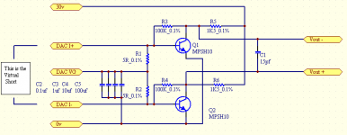
Here is my first bread board draft.
The power supply is meant to be floating compared to the DAC supplies.
The virtual short is between DAC I+ & DAC I-. As for the DAC VG (virtual ground), It may be useful to connect to so some DACs VG's, or the DAC's may perform better without it.
For the DAC's with Voltage out, add a series resistor on both DAC Vouts (+/-) & connect them to the DAC I(+/-) on this circuit.
The outputs still need to be buffered. I making a 4 JFET solution which connects right to this design & it will create both Balanced & Unbalanced outputs.
Attachments
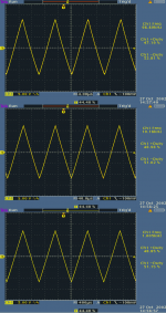
Here are the first tests.
Test equipment:
Lousy BK Precision 3011 function generator.
Good BK Precision 1786 DC Regulated Power Supply.
Great Tektronix TDS 3054 DSO
The scope was operated from battery pack & it was floating.
The DC supply was also floating.
The function generator's ground pin was cut & it was also floating.
For these readings, the source current was at 6.666ma p-p.
A triangle waveform was chosen to verify linearity.
The output voltage is a little overkill, to fix this, R1 & R2 just need to be lowered to 2 Ohm, or 1 Ohm making a terrific virtual short.
Sorry for the squished/scaled scop shot, forum maximum size was reached...
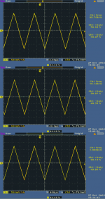
Attachments
Now, to make this design using matched transistors.
I've chosen Analog Devices MAT-04 device.
http://products.analog.com/products/info.asp?product=MAT04
Having 4 transistors will give 2 for the left channel & 2 for the right. In my next drawing, I'll also add an output gain trim & balance.
Now for the Voltage follower / unbalanced conversion stage, if I could only find 4 matched N-Channel J-Fets.
Comments?
hatasa Wrote: (on my dual transistor page)
diyAudio Prophet
------------------------------------------------------
Hi Brian,
I would like to know is it possible to connect with the +/-15 supply.
And I would like to ask is the Vout in balance mode if I connect the GND to VGGND?
-------------------------------------------------------
1. Yes, as long as this supply is floating. The problem here is the location of the DAC's 0 current. My DAC_VG is balanced right between the 2 transistors BASEs. If you were to power this design with my 0v at -15, the DAC-VG will be at around -14.3 volts.
2. With the +/-15v supply & balance calibration, the GND should be fine for the frame ground of output. Yes, this output is balanced.
My additional JFET buffer solution also does a sum inversion improving further the output SNR & it can then be used for both balanced & unbalanced. It also created a new shield GND for balanced.
Using just 2 JFETS, 1 for + & 1 for -, or none at all, now rely's more heavily on you amp's / pre-amps CMRR.
For pure minimalist design, if you want to drive a pre-amp directly, no buffer, in place of the MPSH10s, use the dual transistor LS325A, & shrink R3, R4, R5, R6 so that the circuit will draw 100-200ma across v+&v- instead of the 20ma in the current design. Also, increase C1, the gain BW of this new configuration with C1 at 15pf will be in the 100MHz range.
Which DAC are you using.
Typically, the DAC - input should go to your DAC common, the DAC I output should go to the DAC + input. My DAC VG input should not be used. Remove the C2,C3,C4,C5. R1 & R2 may be replaced with 1 resistor.
A good minature way to test this circuit with an existing DAC PCB would be to power it with 2, or 3 x 9v batteries.
After analysing many dual transistor data sheets, I've determined that Analog Devices' MAT02 dual transistor will incredible preformance & balance in this circuit. In fact, over 20x beter than anything else.
http://products.analog.com/products/info.asp?product=MAT02
Expensive though.
I have the PCM 1704 DACS. they don´t have a balanced output and they have a current output , so I need a I/V converter.
promitheus
Why don´t you try the one Jocko suggested recently.
Haven´t built it myself(yet) but it looks interesting.
Jocko´s I-V stage
Nicke
Why don´t you try the one Jocko suggested recently.
Haven´t built it myself(yet) but it looks interesting.
Jocko´s I-V stage
Nicke
promitheus said:I have the PCM 1704 DACS. they don´t have a balanced output and they have a current output , so I need a I/V converter.
This is an I/V converter.
I assume you mean a Burr-Brown PCM1704. I have never used the component, but I took a quick look at it's data sheet.
For this DAC, I would connect my DAC I- to the ADC's AGND. The DAC's current output should go to my DAC I+.
Set up the PCM1704's (Ref DV, Servo DC, &, BPO DC) so that the Iout from the DAC is biased at the Agnd. Just use they typical application circuit in the data sheet.
Now, the PCM1704's output current on the spec sheet is +/- 1.2mA. This means it is 2.4mA p-p. My R1&R2 @ 5 ohm should be perfect the way they are.
Remember, the output of my ciruit is balanced, even though the output of the PCM1704 is not.
I know this is an I/V circuit, sorry to show I didnt get that in the first place. I only was talking about this DAC, that it needs an I/V converter.
It is a Burr Brown PCM 1704.
and you are right about the specs. It has +/- 1.2 mA.
I think the circuit is typical with REF DC (pin 19) and Servo DC (pin 17) coupled to -5V supply in series with 47uF caps and BPO DC (pin 12) to +5V with 100uF cap.
AGND (pins 15, 16) at ground.
The original circuit has an opamp and I want to get rid of it.
I think a simple circuit will sound better.
So you mean to use DAC I+ and DAC I- as signal and ground.
and what do I do with the ground in your circuit ?
Leave it floating or what should I do ?
Do you have any ideas on what I can do for filtering ?
Both DAC I+ and DAC I- are driving current into a point V<sub>BE</sub> above ground. That seems non-ideal.
Correct. This is why the 30v, or +/- 15v supply needs to be isolated from the dac's supply.
This idea here is to create a minimalist, only, 2 transistor gain stage.
This idea here is to create a minimalist, only, 2 transistor gain stage.
Virtual ground?
Uh.......seems to me that it has 0.7 V DC on it. Do you really think that your DAC is going to like that?
Jocko
Uh.......seems to me that it has 0.7 V DC on it. Do you really think that your DAC is going to like that?
Jocko
Re: Virtual ground?
Correct. This is why the 30v, or +/- 15v supply needs to be isolated from the dac's supply. In other words, FLOATING!!!
YES, A SEPARATE DEDICATED TRANSFORMER, or ISOLATED TRANSFORMER TAP. This 0.7v to the dac will appear to have no current in any direction.
Otherwise, you would need to add a third transistor & diode to drive the emmiters on Q1 & Q2 at the DAC's so that they are 0.7v lower than the I-dc reference of the DAC. The separate supply allows the DAC I to be anywhere & it's load will be balanced dead on. This removes additional calibration of the circuit.
Minimal transistors is the theme of this circuit.
Jocko Homo said:Uh.......seems to me that it has 0.7 V DC on it. Do you really think that your DAC is going to like that?
Jocko
Correct. This is why the 30v, or +/- 15v supply needs to be isolated from the dac's supply. In other words, FLOATING!!!
YES, A SEPARATE DEDICATED TRANSFORMER, or ISOLATED TRANSFORMER TAP. This 0.7v to the dac will appear to have no current in any direction.
Otherwise, you would need to add a third transistor & diode to drive the emmiters on Q1 & Q2 at the DAC's so that they are 0.7v lower than the I-dc reference of the DAC. The separate supply allows the DAC I to be anywhere & it's load will be balanced dead on. This removes additional calibration of the circuit.
Minimal transistors is the theme of this circuit.
Minimalist approach?
I suspect you enjoy doing things the hard way, just to say it is "minimalist". Minimalist does not automatically imply better.
And everything in else in your system after the I/V is going to run off off this isolated supply. No way it is going to be accidentally connected up to the other ground.
And you will get distortion figures approaching -80 dB, right?
But what do I know............
Jocko
OK
Just don't be too disappointed with it. Have you actually made any measurements on it? Not sure what all those pics are. (Hard to read on my screen........)
I would imagine distortion for that type of circuit will be around -40 dB.
Jocko
Just don't be too disappointed with it. Have you actually made any measurements on it? Not sure what all those pics are. (Hard to read on my screen........)
I would imagine distortion for that type of circuit will be around -40 dB.
Jocko
I'll know when I make a DA board with an AD1955 in mono mode, MAT02 for the IV stage, & Interfet's 2N3954 for the CMR line out buffer.
Brian, why don't you think like this (like me): AD1955 is along with a few other chips top of line at the moment. How do I make a nI-V converter which adds NOTHING to the output of the DAC? Isn't this the first question you must ask yourself? I think an AD1955 deserves the best interface to the analogue world. Then I the question comes: Is it possible to make it simple or is a complex circuit neccessary?
- Status
- Not open for further replies.
- Home
- Source & Line
- Digital Source
- A single supply, 2 transistor DAC-IV stage.