Hello bogdan_borko,
An interesting and possible diyF8 candidate. It has a power output stage like J2 per the recent and valuable hint by Mr. Pass, plus loop feedback. More food for thought.
I am inclined to use ACA as a framework to a diyF8; with a modification at its input. I'll work on a plausible schematic.
Best
Anton
From the description of mr. Pass I guess that's it (more or less), simple 3 transistor circuit... (forgot one cap on the mu follower).
Last edited:
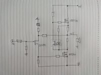
diyF8 via ACA
The attached image has two potential diyF8s which are based on Amp Camp Amp [ACA].
The schematics are separated by a vertical three-line barrier. Each schematic is further sliced therein with a vertical two-line barrier.
Left schematic.
1. The circuit to the right side of the two-line barrier is mostly that of ACA, with several missing [not needed] components.
2. The circuit to the left of this barrier is the modification.
3. I reversed the voltage of the 19 V SMPS so as to reference the input signal to ground for the front end LSJ74 P-FET.
4.The source port of LSJ74 has a degeneration power resistor of value ~1 Ohm or less.
5. The top part of the mu follower connects to the source of LSJ74.
6. The load at the drain of LSJ74 goes directly to the gate of LSK170A which is part of parent ACA.
** The connections in points 5 and 6 above generate a valuable AC and DC "loop feedback". DC feedback stabilizes quiescent conditions. N-MOS is protected by the mu follower [special active load] and from this DC Servo-like feedback.
7. The sum value of the two load resistors at the drain of LSJ74 need to generate a voltage at the gate of LSK170 so as to give it a source current of 4 mA [as in ACA] to bias N-MOS at a Vgs = 4 V.
Right Schematic.
1. All of the above apply to it.
2. The power output stage uses SJEP120R100 [R100] enhancement N-JFET instead of N-MOS. Its operating Vgs is ~1.2 V. I kept a 4 mA source current for LSK170. Thus its new gate voltage must be adjusted by a new sum value resistors.
3. Why R100? It has a lower gate capacitance than N-MOS. It may not need the preceeding LSK170 buffer. Thus, it'll be a direct drive to the gate of R100 from the adjustable load resistors of LSJ74.
Questions?
Is ACA an H2 Power Generator?
Is the H2 from ACA "pure"?
Best
Anton
Attachments
Last edited:
A diy amp with no name
It is a simple prototype amp. It sounds great. It is an H2 power generator. This is evidenced by its two different sounding music by way of reversing the loudspeaker leads. Mr. Pass taught us this simple method to differentiate -H2 from +H2.
The attached image shows the 3 steps I used to design the amp.
STEP #1.
I have two matched LSJ74 P-JFETs. I measure Idss for each [~10.5 mA]. I connect them in parallel to get ~20 mA. They share equally this resultant net Id which I show as a voltage drop across a 10 Ohm.
STEP#2
1. I used a 15 Ohm source degeneration resistor [by trial and error] to cause a new net Id ~10 mA. This centerpoint Id can be coached by the music signal to increase to +19 mA [close to Idss] and decrease to 1 mA [close to cutoff].
2. The net drain current [10 mA] is equal to the net source current flowing through the 15 Ohm degeneration resistor. The resultant voltage drop across this resistor is ~150 mV. This voltage drop drop is important.
3. I divide this 15 Ohms by 100 to get 0.15 Ohms. This 0.15 Ohm is a power resistor made by paralleling 0.2 Ohms and 0.5 Ohms.
STEP #3
1. The original 15 Ohm degeneration resistor for P-JFET is now 0.15 Ohms.
2. A ~1 Amp current flowing through this 0.15 Ohm resistor develops a 150 mV voltage drop across it. This is the induced drain current of IRFP140 which is a power N-MOS.
3. This resultant 150 mV voltage drop [externally induced] instructs P-JFET to generate its net drain current of 10 mA as determined in step #2.
4. This Id of 10 mA flows thru an adjustable 490 Ohm load resistor [390 Ohm and 100 Ohm multi-turn pot]. It generates a Vgs = 4.1 V for N-MOS which pulls a ~1A across the 0.15 Ohm degeneration resistor of P-JFET.
5. The input gate capacitance of N-MOS is 2800 pF. An NPN buffer is used to drive it.
6. The amp sounded well by driving N-MOS without NPN.
7. The load to N-MOS is a 10 Ohm /40 W resistor. I adjust the 100 Ohm pot [point 4] so as to divide equally the power supply voltage of [-20V] between the 10 Ohm load and NMOS.
To be continued...
Best
Anton
Attachments
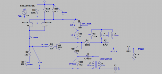
The Power of Degeneration
The schematic of today's prototype amp shows a 0.5 Ohm degeneration resistor at the source of N-MOS power output generator.
Wow! It dramatically improved the musical performance of the recent prototype; which has an absent degeneration resistor.
The value to performance of including a degeneration resistor is well established. It causes local negative feedback so as to:
1. Stabilize the direct current flowing thru N-MOS.
2. Reduce the harmonic distortion of N-MOS.
Without this degeneration, the burden to stabilize drain current and lower N-MOS distortion is the full-time job of P-JFET. P-JFET is an error amp. It compares the music signal at its source [from N-MOS] with the pristine input signal at its gate. The net result is an error signal which is presented to the gate of N-MOS so as [via phase inversion] to counteract its distortion and stabilize its drain current.
The 0.5 Ohm degeneration resistor has reduced the burden on P-JFET to correct the errors of N-MOS. It practically clarified the musical performance. I was astonished!
The schematic of this new prototype amp [still with no name] is attached. It is thermally stable and against oscillation.
to be continued..
Best
Anton
Attachments
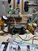
Where's the beef?
The image of the prototype [beef] is attached.
1. IRFP140 is on the left heat sink below 2N3055. The 0.5 Ohm degeneration resistor and a protection Zener [8.4 V in pill container] are below it.
2. The 10 Ohm load resistor is clamped on the right heat sink. It does not have to; because it only idles at ~10 W and is rated at up to 40 W. But it gets scolding hot! I am using steel wool [non-shedding] to couple its irregular flat structure to the sink for best heat transfer.
" CAUTION": Steel wool ignites and bursts into flames upon passing a current through it. This is practiced by scouts to start a camp fire with AA battery.
3. The input P-JFETs and NPN buffer are shown on the upper left side of the protoboard. Above it are the remaining inter-connected components.
to be continued..
Best
Anton
Attachments
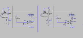
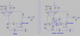
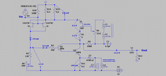
Another pair of diy amps with no name..
I used two Depletion JFETs [LSJ74 and SJDP120R085] in this prototype. This is shown in the image of the dual and related schematics.
Left-side schematic.
1. The use of SJDP120R085 [R085] required the use of an additional -5 V PSU so as to bias its gate more negative than its source. Its connection is encircled at the bottom of the schematic.
2. Sounds great.
Right-side schematic.
1. I inserted a non-inverting Opamp [OPA134PA] gain unit in the loop. Its AC gain = 1.6 from {1 + [8.2K/15K]}. Its DC gain equals 1 because the inverting port is AC coupled to -5 V rail.
2. Prone to spontaneous oscillation at higher gains of OpAmp. The OpAmp is implicated for this behavior. Because of its high open loop gain, and it does not like to drive the input gate-source capacitance of [R085].
3. The increase in power output gain is perceptible. Simply disconnect the blocking 2uF cap from the - 5 V rail. Now, the OpAmp works as a unity AC and DC buffer. This action effects a loss of output volume.
4. Still sounds great
Best
Anton
Attachments
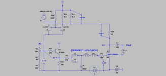
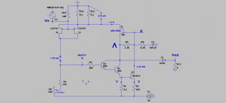
Another power amp
Some of you may like to pass the music signal through "iron". This amp is agreeable to this.
The attached image of the prototype amp shows:
1. A Jensen JT-123-FLPCH transformer [from the fame of F6] is used like done by Mr. Pass in M2, DEFiSIT etc. The music signal is actually passing through an alloy of Iron/Nickel.
2. This arrangements of the transformer injects a gain of 2 times inside the loop.
3. 2N3904 [enhancement BJT] forces the use of a higher-valued load resistor to the front-end LSJ74. Gain of LSJ74 is proportional to its load resistance. Thus, this arrangement adds more intra-loop gain; by a factor of maybe 0.45 from the ratio of the added 82 Ohms [to bias BJT] divided by its sum of 180 from the original 100 Ohms [no BJT].
4. The use LSK70 [depletion] in place of 2N3904 buffer removes gain from the loop. Because; the original 100 Ohm load resistor to LSJ74 [absent either buffer] must be reduced further to properly bias R085 to the same Vgs =3.7 V.
5. The value of increasing intra-loop gain as above lowers distortion and output impedance of this power amp.
Best
Anton
Attachments
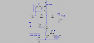
A signal-modulated load
The attached image shows an incomplete schematic of the subject load. Here are its salient parts:
1. UJN1208K power depletion JFET is the variable load to Darlington bjt. The 4 Ohms/20 W resistor at its source establishes a Vgs = 4 V and/or an idle current of 1 A flowing through it [Ids] and through the collector of bjt.
2. A toroid transformer is used to generate the modulating signal which goes to the gate of UJN1208K
3. Why a toroid at this juncture? This toroid gives many specific transform ratios from step down [X 0.25] to step up [x10] ratios; so as to determine the best magnitude signal for presentation to the JFET's gate.
4. The image shows the coupling toroid as a 1:1 transformer.
5. The degeneration resistor [0.2 Ohms] at the emitter of bjt drives the primary winding of the toroid. The back and forth music current which flows through this degen resistor has the same magnitude as the current flowing throuh the loudspeaker.
6. The toroid's primary winding is out of phase with its secondary This arrangement speaks to defining the direction of the current flowing through the degen resistor or through the loudspeaker.
7. The music signals at the gate of JFET and Vout [bjt collector] are in-phase. Music sounds best with this arrangement versus the out-of-phase condition.
To be continued..
Best
Anton
Attachments
Prototype amp utilizing a signal modulated load.
The attached image is the schematic of a single-ended proto-amp understudy. The Darlington gain transistor uses its internal process signal to modulate its load.
Modulation changes the conductance of UJN1208K [1208K] in these specific ways:
1. Conductance of [1208K] increases when the relative phase of the output AC signal [Vout] is positive-going. This is needed to drive the loudspeaker with more current because BJT's conduction is decreasing.
2. Conductance of [1208K] decreases when the relative phase of the output AC signal is negative-going. Its current's contribution to the loudspeaker decreases [not as needed] because ground [common] now supplies the needed current which is demanded by BJT.
My simple definition of modulation is the ratio of the AC voltage at the gate or the source of [1208K] to Vout. The toroid is the generator of the modulating voltage at the gate of [1208K]. The salient details of the toroid circuit are:
1. Its primary windings [2 parallel 2 Vac] sample the total current flowing thru the loudspeaker and its phase.
2. Its secondary windings [2 series 115 Vac] drive the gate of [1208K] via a tunable 25 K linear pot.
3. The maximum voltage step-up ratio for this toroid is [230/12 =19]. I measured ~18.
4. The wiper of the 25 K pot was set half way and goes to the gate of [1208K].
5. The modulation ratio is equal 1/2 for this arrangement. May need further tweaking to maximize Vout. In general, Vout increases with increasing modulation ratio. I'll find the peak Vout.
This proto-amp sounds great. It's quiescent conditions are stable and does not oscillate.
To be continued..
Best
Anton
N.B. Error correctin in schematic:
The secondary windings of the toroid must be connected in series instead of parallel as shown
Attachments
Last edited:
Simplify prototype....
I eliminated the toroid and the 4 Ohms/40 W resistor at the source of UJN1208K [1208K] in the schematic of the last post. Both components had helped my understanding of this modulated load understudy. It is still being tweaked.
The attached schematic shows:
1. A low power JFET [2N3819] is used as a constant current source [1.24 mA] to bias [1208K] ~1A drain current at idle. The magnitude of its Vgs ~4.1 V which was developed across the 3.3 K resistor between its source and gate.
2. JFET [2N3819] is also used to modulate the gate of [1208K]. It operates like BJT; albeit as a low power phase inverter of the signal at the degeneration 0.2 Ohms resistor; for presentation to the gate of [1208K].
[3]. The phase of Vout at the source and gate of [1208K] are the same. Except, the signal at Vout is larger in magnitude than the signal at its gate. This was done by using the 8.2 K in series with 100 uF to ground [shunt] at the gate.
[3a]. Gain is greatly maximized when the gate shunt is removed. The modulating signal at the gate is now higher in amplitude than Vout.
[3b]. Thus, the gate shunt [specifically its resistor value] allows to vary modulation.
4. An AC signal at the drain of [1208K] signifies its modulation.
5. How about operating "push-pull"? Still unclear.
This prototype amp sounds great driving a 8 Ohms Karlson.
to be continued ..
Attachments
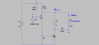
Refining the prototype
The attached image shows a simplified schematic of the refined prototype understudy. Please note the following:
1. My past prototypes always showed a connection of the "Black" loudspeaker lead to ground/common. Not anymore!
2. This schematic shows the "Black" lead of the loudspeaker still goes to ground; except via the 0.15 Ohms degeneration resistor at the source of PJFET.
3. The music current which flows thru the loudspeaker may be understood as total current feedback to the frontend PJFET. It develops a feedback signal [V feedback] across the 0.15 Ohms degeneration PJFET resistor. PJFET then compares the pristine [Vin] at its gate with the recycled [V feedback] at its source. Thus, PJFET generates an error signal at its drain which drives the base of BJT. This error signal is amplified and phase inverted by BJT such that it nulls the distortion at [Vout].
4. Sounds great.
5. Its operation; meaning the current flow of the music signal is understood by you all. Was not evident to me; but I'll explain in the next post.
Best
Anton
Attachments
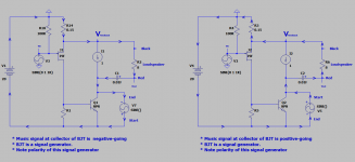
The attached is a split-image of the prototype understudy. It explains how the amp works. It maybe less than be "rigorous"; but it works as follows:
1. The constant current source [ccs] cooperates with BJT to make it a power signal generator.
2. The left-side schematic shows the flow of the music's current when the signal voltage at the BJT's collector [Vout] is negative going relative to idle state.
2a. The music currents starts its journey at the anode or positive junction of this generator [emitter of BJT].
2b. The music current meanders in the circuit to finally returns to the cathode of the signal generator [Vout] where it belongs.
2c. Notable [the intention] is the music current flows thru the degeneration resistor [0.15 Ohm] at the source of PJFET [for error correction] and thru the loudspeaker.
3. The right-side schematic shows the flow of the music current when the signal's voltage at BJT's collector is positive going.
3a. The resultant music current starts its flow at BJT's collector [anode], passes thru the loudspeaker and the degeneration resistor and terminates atr BJT's emittor [cathode] where it belongs.
And thus, the music [alternating] current makes a full cycle thru the loudspeaker.
The power source [VA] for BJT is the [ccs] and ultimately the main 20 V power supply.
to be continued..
Best
Anton
Attachments
- Home
- Amplifiers
- Pass Labs
- A Simple Power Amp