This simple prototype amp also has a wow musical performance.
Here is an introduction to its evolution:
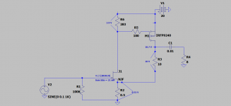
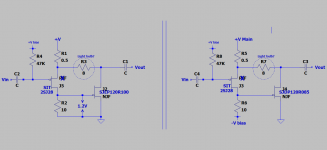
1. Start with the schematic of a diyF5.
2. Slice it along a horizontal line which passes through the input port, along the feedback resistor and the power output.
3. Two independent power amps are obtained. The schematic of the upper half-slice is attached. Isn't it very simple! Per Mr. Pass, best musicality is commensurate with simplicity.
I look forward to your posts.
Best
Anton
Here is an introduction to its evolution:
1. Start with the schematic of a diyF5.
2. Slice it along a horizontal line which passes through the input port, along the feedback resistor and the power output.
3. Two independent power amps are obtained. The schematic of the upper half-slice is attached. Isn't it very simple! Per Mr. Pass, best musicality is commensurate with simplicity.
I look forward to your posts.
Best
Anton
Attachments
The F5 is actually two single ended amplifiers connected in parallel. That's why you can slice it in two.
Just need to scale down the NFB network to take the DC bias current, and add the output coupling capacitor.
Just need to scale down the NFB network to take the DC bias current, and add the output coupling capacitor.
Last edited:
Thanks rayma for your post.
The amp's psu must be robust and especially clean. P-MOS appears as a common gate which will pass noise into the load.
The input N-JFET is a parallel of 4 [2N3819]. The Idss of each FET is roughly 5-6 mA at a 12 Vds. They'll share ~equally the net sum Idss = 21 mA.
In operation, Ids of the NFETs drops to ~13 mA. It can swing up to 20 mA and drop down 6 mA. This span is needed to drive P-MOS for output power.
Best
Anton
H2 Power Generator
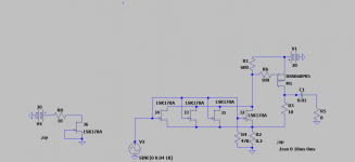
The Simple Power Amp is also an H2 power generator. I've attached an image of a simple SPICE model which is like the schematic I showed in post #1. You folks can do much better than me to improve it and its performance.
Its FFT is rich in H2, H4 and H3. Also, its frequency range [5-80 KHz] appears to be "clean" of harmonic hash.
Mr. Pass had mentioned [somewhere] that the power output of his upcoming F8 is rich in H2 and its FFT spectrum is "pure".
Does "pure" mean "clean" of hash?
Is the schematic/prototype I have presented a candidate diyF8?
The good news is this topology has many "viable candidates".
I'll tell you more about the its broad scope of application.
Best
Anton
Attachments
Oh.
I remember Papa revealed quite a bit verbally.
I will have to find it.
I will sleep first though.
I remember Papa revealed quite a bit verbally.
I will have to find it.
I will sleep first though.
Schematics of H2 Power Generators
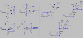
tweakPlease see the attached mosaic of schematics for H2 power generators. It is a broad scope.
Note the following:
1. The schematic with a [*] on the right side of the vertical 2-line barrier. It is the upper one I sliced from diyF5 in post#1.
2. The schematic with a [*] on the left side of the barrier is the compementary symmetry topology of the one in post#1. It is the bottom slice of diyF5.
3. The schematics containing [T for tried] were assembled and assessed for musicality. I will qualify [T for tried] in future posts by showing the actual schematics used.
4. The uniqueness for the power output semiconductor gave diverse schematics. Performance is expected to be different among the devices; because each has a unique structure-composition.
N.B. Please see post#8 by Mr. Pass. He narrowed possible candidates [if so] to the schematics which are on the left side of the vertical barrier.
Best
Anton
Attachments
Last edited:
F8 is a P followed by an N
I posted this in January of this year as an all-SIT two-transistor concept.
Attachments
A plausible candidate. Did you prototype and listen to it?
I wish. I am on the work version jury duty. All day meetings for the entire summer. The good news is that I may get a new toy as a result.
Concept diyF8 schematics
The following concepts were directly spurred by hints on F8 by Mr. Pass in past threads [this forum] and/or YouTube.
F8 is a simple amplifier and a"pure" H2 power generator.
The attached schematics were my initial theoretical diyF8s. Educated guesses at best! The three candidates fit the description in post #8 by Mr. Pass. But they also need to be practical!
Please note the following:
1.The left-side schematic uses a front end P-JFET; like LSJ74, or its several parallel units. They are available in our diyAudio store. I have 4 2SJEP120R100 [R100] enhancement N-JFETs from the good older days of diyF6.
2. The right-side schematic is a dual. Its left schematic uses a front end P-VFET [2SJ28], and a power output R100. This combination shows a P-depletion followed by an N- enhancement unique devices. Note the added complexity of adding an independent bias to the gate of 2SJ28. Please note the "lightbulb" load to R100. I was thinking of Mr. Rothacher's: L'Amp a simple SIT.."
3. The furthest right schematic use two depletion devices. Clearly different from candidate in #2. Note the added complexity of adding another bias power supply for the gate of power output SJDP120R085 [R08]. I have 3 R085s from the good older days of DEF.
I get the sweats before I power up any amp which uses VFETs. The resistance of its Drain-Source is a dead short. It could be damaged permanently. But, this diyF8 topology which uses VFET as a front end and an enhancement device as power output PROTECTs this vulnerable device. This is because of the "loop feedback therein.
Like this: As the conductance of the front-end P-VFET increases, its output current simultaneously increases the conduction of the enhancement device. But the resultant output current of the enhancement goes to the source of VFET; which drives it more negative [relative to the positive gate] so as to decrease its conduction.
Please play this game with a diyF8 using the 2 depletion devices.
Best
Anton
Attachments

This is what I've been building for a while. Nice measurement result and nice sound. I think P to N is promising. 🙂
All SIT 50W+ Single Ended Amp (beta)
All SIT 50W+ Single Ended Amp (beta)
Hello plasnu,
Interesting design. Its complementary symmetry: N first [2SK82] and P out [2SJ82] may also work. I worry about high voltage [220 Vdc] in diy projects. Can you lower the magnitude of the PSUs to safe levels? Is a higher current and lower voltage design an alternative.
Interesting design. Its complementary symmetry: N first [2SK82] and P out [2SJ82] may also work. I worry about high voltage [220 Vdc] in diy projects. Can you lower the magnitude of the PSUs to safe levels? Is a higher current and lower voltage design an alternative.
Last edited:
Antoinel, it is 320V now. If we use choke for 2SJ28, the voltage can be much lower. Low voltage/high current setting can't make 2SJ28 swing a lot. High voltage for voltage gain, high current for current gain is my natural choice here. 🙂
Bias scheme is still changing, so I'll update the schematic soon.
Bias scheme is still changing, so I'll update the schematic soon.
US 5,710,552
It is your subject patent. By example, the power output stage of ACA.
The F8 output device is biased by a mu follower, just like the J2.

It is your subject patent. By example, the power output stage of ACA.
Attachments
The F8 output device is biased by a mu follower, just like the J2.
Hello Mr. Pass,
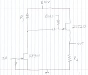
The attached schematic is for a prototype diyF8 I had assembled. I used therein an active load to the power output NPN [2N5301]. It is encircled.
This active load biases NPN at ~a 1A collector current. But; is it a mu follower or just a generic active load? Please advise. Thanks.
Attachments

- Home
- Amplifiers
- Pass Labs
- A Simple Power Amp