hope you are doing fine leventi !!!!
I hope the same for you and... for me! 😀
Thanks by anyway patrida.
I recommend the extra resistor from supply rail to protection transistor base to bring in the V part of the VI limiter.
Leach omits it, but the Leach clone has it in place. Many other designers use this version of the VI limiter.
Leach omits it, but the Leach clone has it in place. Many other designers use this version of the VI limiter.
very nice fotios .... as i said above the vi limmiter is to be constructed in the next few days it will be more than that ... and a a lot more to talk about
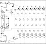
But here is a an interesting question :
the limiting transistor effects through the diode in the base of the driver transitor ...now behind the base of the transitor there is a resistor of 100R some apply the limit before the resistor and some after
to my understanding if you apply the limmit after the resistor and directly on the base of the driver then the VAS will have an easier Job to do please correct me if am wrong ...
then gain sensing from all power tranistors is something i wouldnt like to do ...Last night i designed a new pcb ( again!!! ) that comed in very very comapct i noticed a problem such : rail suplly will be ideally in the midle point between the 5 transitors per rail .... now in my pcb the distance from transitor 1 to transistor 5 is bearly 10cm and the trace is 4.6mm wide and it will be also propely thicked .... but still power will be applyied
in the side and not in the midle .... no mater how thick is the trace it is obvious that transitor #1 that is most far away from the rail supply will have the most stress ...so sensing from there only will be enough for me ...
please comment
It certainly helps.the limiting transistor effects through the diode in the base of the driver transistor ...now behind the base of the transistor there is a resistor of 100R some apply the limit before the resistor and some after
to my understanding if you apply the limit after the resistor and directly on the base of the driver then the VAS will have an easier Job to do please correct me if am wrong ...
A 50V supply feeding through VAS to 100r to the saturated protection resistor into an output rail that could be anywhere between +49V and -49V is a might big current. Worst case is 1Apk. Bye bye VAS.
Without the 100r the peak current could be even worse.
The VAS must be current limited if protection like this is adopted.
A VAS emitter resistor of 24r would be about right for a 50mA 5W VAS biased to <=8mA fed from +-50Vdc
Last edited:
ok ...this is what i thought also ....
your comment might be correct at dc conditions and given as a fact that
---- full signal is supplied
---- output is shorted by all means
---- then protection is active and Vas is loaded
but in music , reactive load , transients and peaks you might get away with it
will test and get back to you about this one
regards sakis
to get protection operating with the output @ 99V relative to VAS there must be a high signal level and there must be a reactive load, not a short circuit.
This overload condition will definately be very short term.
But, I would never design for 1Apk passing a 50mA device, not even a 100mA nor 150mA device.
If the output is shorted, the output rail must be at or very near 0V. Then the worst case VAS voltage is ~50V. I still would not design for 500mA through a 150mA device for 100ms.
- Status
- Not open for further replies.
- Home
- Amplifiers
- Solid State
- A ...power amplifier