While testing and waiting for NP FE 2022, I bought bunch of Toshiba 2SK209GR and BL. By optimized pairing, I got few precision marched 2 quad BL and 2 quad GR for LTP with Idss 19mA and 10mA. Then I though why not paring one BL and one GR to get a Idss 14mA device. So I did and plotted the Id-Vgs curve. Now I have 5 devices for the LTP with different Idss and gm. The left is dual BL on Al PCB. The green one is quad 2SK209GR or 2x(BL+GR). There are two Jfet on the back side.
By watching the curve, I saw a point. What could happen, if we set LTP Id at 2mA and Vgs at -0.5V? Then on the negative signal, only BL works, GR has very little current. On the positive signal, both work and Id follows the new BL+GR curve. We Could get more distortion. What could we get?


By watching the curve, I saw a point. What could happen, if we set LTP Id at 2mA and Vgs at -0.5V? Then on the negative signal, only BL works, GR has very little current. On the positive signal, both work and Id follows the new BL+GR curve. We Could get more distortion. What could we get?
Last edited:

I don’t have the models for 2SK209GR and BL, so I use J113 and J112 to simulate it. For the models used, Vgs around -1.2V, Idss around 4.5mA is the wished working point.

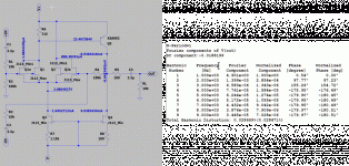
Pass original FE 2022, CCS same, change one J113 to J112, R6 value to get comparable DC offset at output. Total THD increased, but it is H2, H3 decreased.

Modified CCS to the working point shown before, 4.5mA each side Jfets, 1.2V Vgs. Total THD further up, H2 further up, H3 further down.

Summarized in a graph.
Vp and Idss of J112 are too large, combined with large Idss of J113, the combination of J112+J113 does work well in Pass FE2022. Also when output increases to 20V and 40V pp, it simulated more H3 than the original. Because of a limited voltage drop on R6, I have to reduce it when the Id and Vgs have to be set to the special point. This reduced the OLG of the circuit. So higher total THD.
If we stick to the CCS of Pass’ circuit, 2SK209BL+GR might be a suitable solution.
This is just theoretical. I don’t have proper equipment to test this concept but my ears in the future.
Last edited:
Sweep Vgs from -6V to 0V (DC analysis) and plot the square root of IDS. Do this for three different "Device Under Test": 209-GR , 209-BL , (1_of_GR parallel 1_of_BL).
Are any of them remarkably more smooth (or remarkably less smooth) than the others? Anything that looks like it might provoke or prevent nonlinearity & distortion?
The modeling equations built into LTSPICE insist that Ids is proportional to the square of (Vgs - Vpinchoff), which is why we take the square root when plotting.

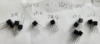
In practice, we could use two J113 instead of J113+J112. I bought 100 J113, Idss is from 20 to 28mA. The majority is in 24-26mA.
I picked two of them. One(#2) has Idss 23.3mA, Vgs(off) -2.1V, and another(#3) 27.6ma, -2.38V. The Id vs Vgs curve of 2xJfets and #3+#2 are shown.
Assuming we don’t change R6 680 in NP FE2022, the Id from each side is est. 0.9mA if the offset should be decent. For 3 devices used in LTP, the Vgs is shown(-2.2V, -2.1V and -1.92V).Then we change Vgs +/-20mV around the this point and the Id change can be estimated and so the gm in +signal and –signal. The ratio of gm of +/- signal around the working Vgs are 1, 1.32 and 1.14.
So could we say, when double Jfets for LTP, Jfet has different Idss and Vgs(Off) could be used. To max H2, the working Vgs of one Jfet should be near its Vgs(off) and Id of another Jfet should be near the setting value at Vgs(off) of the first Jfet.
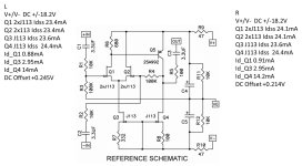
This is the DC operating points of NP 2022 FE with the Store Kit with +/-18VDC power supply.
Attachments
Last edited:
- Home
- Amplifiers
- Pass Labs
- A possible new method to enhance the enjoyment of Pass FE2022