Note:
The title should be:
A linear regulator circuit to help me understand since I make too many errors in predicting circuit behaviour.
I am posting to this sub-forum because my goal for this thread is to help me clear any misunderstanding I may have regarding the use of differential pairs. Yes, I used a differential pair in my amplifier project, and it works, but going the learning path higher up, is an exciting journey I would like to try.
The content and question:
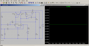
The circuit is a series pass regulator I designed. Under LTSpice it looks it is a good regulator that can tolerate power supply variations beyond -50%. It also provides the ability to select an output voltage down to 0V. It uses a voltage reference, a differential pair and a series pass Sziklai connected transistor pair.
This is my inexpert reasoning of the circuit:
A differential pair works best if both transistors carry very nearly the same current. I provided for this condition by using two 1k biasing resistors from the bases to ground. This bias provides the stable component of current to the differential pair. Using two equal resistors ensures both transistors are equally driven. To provide signals to the differential pair, I used two 100k resistors. My reason for choosing such high value is not to disrupt the differential pair currents from their balanced values. I connected the inverting input to a potential divider consisting of two equal 470R resistors that is connected to the regulated output. The non-inverting input has been connected to the voltage reference. The Sziklai pair is driven using a current mirror. A current mirror ensures equality of differential pair current and also enables the use of lower supply voltages. This configuration gives an output voltage that is twice the voltage reference. The output potential divider consists of 470R not to disrupt the divider's voltage by the current drawn from/into the 100k resistor.
Please note, I am using a virtual split power supply for this circuit by using a potential divider of two equal resistors with one of them having a 1uF capacitor across. The virtual split supply is required to achieve outputs down to 0V.
Simulations on LTSpice:
The first simulations resulted in a self oscillating circuit. I tried several times to tame this. First, I connected a 1n capacitor between the base and collector of the driver transistor in the Sziklai pair, but this, failed for some reason mysterious to me. Then, I remembered the Blameless Amplifier and tried to mimic it by connecting the capacitor across the base of the driver to the output transistor of the Sziklai pair. This worked.
Note: V(n002) is the regulated output. The output current is around 1A.
The title should be:
A linear regulator circuit to help me understand since I make too many errors in predicting circuit behaviour.
I am posting to this sub-forum because my goal for this thread is to help me clear any misunderstanding I may have regarding the use of differential pairs. Yes, I used a differential pair in my amplifier project, and it works, but going the learning path higher up, is an exciting journey I would like to try.
The content and question:
The circuit is a series pass regulator I designed. Under LTSpice it looks it is a good regulator that can tolerate power supply variations beyond -50%. It also provides the ability to select an output voltage down to 0V. It uses a voltage reference, a differential pair and a series pass Sziklai connected transistor pair.
This is my inexpert reasoning of the circuit:
A differential pair works best if both transistors carry very nearly the same current. I provided for this condition by using two 1k biasing resistors from the bases to ground. This bias provides the stable component of current to the differential pair. Using two equal resistors ensures both transistors are equally driven. To provide signals to the differential pair, I used two 100k resistors. My reason for choosing such high value is not to disrupt the differential pair currents from their balanced values. I connected the inverting input to a potential divider consisting of two equal 470R resistors that is connected to the regulated output. The non-inverting input has been connected to the voltage reference. The Sziklai pair is driven using a current mirror. A current mirror ensures equality of differential pair current and also enables the use of lower supply voltages. This configuration gives an output voltage that is twice the voltage reference. The output potential divider consists of 470R not to disrupt the divider's voltage by the current drawn from/into the 100k resistor.
Please note, I am using a virtual split power supply for this circuit by using a potential divider of two equal resistors with one of them having a 1uF capacitor across. The virtual split supply is required to achieve outputs down to 0V.
Simulations on LTSpice:
The first simulations resulted in a self oscillating circuit. I tried several times to tame this. First, I connected a 1n capacitor between the base and collector of the driver transistor in the Sziklai pair, but this, failed for some reason mysterious to me. Then, I remembered the Blameless Amplifier and tried to mimic it by connecting the capacitor across the base of the driver to the output transistor of the Sziklai pair. This worked.
Note: V(n002) is the regulated output. The output current is around 1A.
Attachments
Last edited:
Correction:
The above mentioned 'ground' is the virtual ground at the midpoint of the potential divider used to create it.This is my inexpert reasoning of the circuit:
A differential pair works best if both transistors carry very nearly the same current. I provided for this condition by using two 1k biasing resistors from the bases to ground.
...A differential pair works best if both transistors carry very nearly the same current. I provided for this condition by using two 1k biasing resistors from the bases to ground. This bias provides the stable component of current to the differential pair. Using two equal resistors ensures both transistors are equally driven. To provide signals to the differential pair, I used two 100k resistors. My reason for choosing such high value is not to disrupt the differential pair currents from their balanced values. I connected the inverting input to a potential divider consisting of two equal 470R resistors that is connected to the regulated output. The non-inverting input has been connected to the voltage reference...
It is a way to adjust to the virtual midpoint, but given this configuration and the high value resistors, there is some risk of oscillation. 100k / ( 1k + 3k3//3k3 ) is an inner amplification loop of 37.7x, Q2, Q4 and Q3 make the amplifier. Add some extra capacitance (Ccb) to see what happens.
And why so difficult? Why the need to adjust a regulator? Once set, how often you're going to adjust? If it is for a regulated power supply for testing equipment, way better circuits (with foldback protection) are amply available.
How are you going to realise V1? There is no zener working with a 100k series resistor. You will need a regulated power supply for that. Oh...
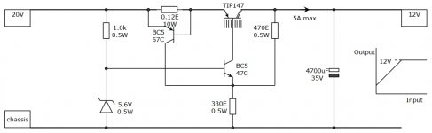
I made an autodrop regulator years ago, with as minimal as possible components and with overcurrent protection.
Attachments
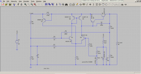
The attachment is the same circuit I posted earlier with added modifications. There is the added use of a voltage reference for the comparator sub-circuitry. Short circuit current limitation has also been incorporated into the circuit. The simulated short circuit current is 3A. The circuit goes down to zero volt output.
The aim of the entire circuit is a variable voltage output that goes down to zero volts. The latter, adds extra complexity.
R14 and R15 are a potentiometer of value 4.7k. Two series resistors were used to simulate the slider action. The total series resistance is 4.7k.
The aim of the entire circuit is a variable voltage output that goes down to zero volts. The latter, adds extra complexity.
R14 and R15 are a potentiometer of value 4.7k. Two series resistors were used to simulate the slider action. The total series resistance is 4.7k.
Attachments
Last edited:
I would like to ask whether balancing a differential pair's current is done in the way I did it. According to my understanding, a differential pair has two components of current, one is a stable bias current, and the other, is the signal itself. The biasing currents must be equal for the best linearity and predictable behaviour.
Is my understanding correct or not?
Is my understanding correct or not?
The output legs of the diff are supposed to be equal for best linearuty indeed, but are tipped off balance by corrective action, that's the goal. The amount of unbalance should not go larger then its long tail current source. With bipolars, unbalance acts exponential. So in short, that's correct.
But how much it is predictable depends on your definition of both the circuit and the word. The circuit is not predictable when the bias is equal alone, it is the complete circuit that acts according to your design and the specs of the components.
What I consider unpredictable concerning the behaviour of the diff is the connection with the overcurrent detector Q7, which will lift both sides of the diff (common mode) until saturation kills the diff operation, leaving the output in one of its ultimate dual states: on or off. Ic from Q7 should switch off Q4 instead, so you need an entry on the diff to do so. That would be Q1 (comparable with my circuit's action on the emitter, whereas the reference side on the base stays equal).