One of my preamps is the DIY Front End 2022 by Nelson Pass (https://www.diyaudio.com/community/threads/diy-front-end-2022.394339/). My other preamp is a CCS loaded Sony 2SK79 single ended circuit (https://www.diyaudio.com/community/...output-triode-like-distortion-profile.386337/). I use both of them with my SIT follower amps. My follower amps range from moderately low power to moderately high power.
My 2SK79 preamp has enough output voltage to allow my amps to output their maximum power into 8 Ohm. However my DIY FE 2022 preamp does not have enough output voltage. Currently my highest power SIT follower can output 70W into 8 Ohm. That requires about a 38Vp input signal (approximately 27Vrms), but the DIY FE 2022 with a 62Vdc power supply can only output a maximum of approximately 27Vp (19Vrms).
The DIY FE 2022 maximum output is restricted by the maximum power capabilities of its transistors, particularly their maximum power dissipation and maximum voltage capability, and by its power supply voltage. Without a higher power supply voltage, a higher output voltage is not possible. So in order to up the maximum voltage output, the power supply voltage needs to be increased and the transistors' maximum voltage and maximum power dissipation need to be increased.
The power supply voltage was the easy part. An 80VDC minimum power supply would be required. 100VDC power supply capacitors would be needed, and I will make adjustments to my shunt regulated mosfet voltage follower power supply.
The next step was to find transistors that are compatible with the higher power supply voltage. Years ago Nelson published this article: https://www.passdiy.com/project/amplifiers/diy-op-amps
Or see attachment below.
It was very informative, and is great reading for anyone who wants to learn about op amps and building discrete op amps. I was able to try some of the transistors that were in Nelson's circuits in my LTSpice simulations.
I tried many versions in LTSpice, and I settled on this:


With an 80VDC power supply, the simulation yielded 37Vp. The simulation distortion numbers my not reflect reality.
To be able to withstand the higher voltage and dissipation, the DN2540 was chosen for CCS duty, with the TO-92 package for M4 and the TO-220 package for M1. The input transistors are ZVN3310, and the output transistor is a BD140 in a SOT-32 package.
One of my big concerns was frequency response, specifically whether the circuit simulation showed a high frequency boost or oscillation. In the end the circuit I chose had a high frequency boost in the simulation, but the addition of a compensation capacitor seemed to tame it. Interestingly I simulated the DIY Front End 2022 in LTSpice and the frequency response plot showed a high frequency boost. However in real life, I measured my build of the DIY Front End and there was no high frequency boost or oscillation. So it remains to be seen whether this design of mine will have an issue or not.
With no compensation capacitor C6, frequency response and 20kHz square wave:


With 500pF compensation capacitor C6, frequency response and 20kHz square wave:


The PCB:

Top copper:

Bottom copper:

My 2SK79 preamp has enough output voltage to allow my amps to output their maximum power into 8 Ohm. However my DIY FE 2022 preamp does not have enough output voltage. Currently my highest power SIT follower can output 70W into 8 Ohm. That requires about a 38Vp input signal (approximately 27Vrms), but the DIY FE 2022 with a 62Vdc power supply can only output a maximum of approximately 27Vp (19Vrms).
The DIY FE 2022 maximum output is restricted by the maximum power capabilities of its transistors, particularly their maximum power dissipation and maximum voltage capability, and by its power supply voltage. Without a higher power supply voltage, a higher output voltage is not possible. So in order to up the maximum voltage output, the power supply voltage needs to be increased and the transistors' maximum voltage and maximum power dissipation need to be increased.
The power supply voltage was the easy part. An 80VDC minimum power supply would be required. 100VDC power supply capacitors would be needed, and I will make adjustments to my shunt regulated mosfet voltage follower power supply.
The next step was to find transistors that are compatible with the higher power supply voltage. Years ago Nelson published this article: https://www.passdiy.com/project/amplifiers/diy-op-amps
Or see attachment below.
It was very informative, and is great reading for anyone who wants to learn about op amps and building discrete op amps. I was able to try some of the transistors that were in Nelson's circuits in my LTSpice simulations.
I tried many versions in LTSpice, and I settled on this:
With an 80VDC power supply, the simulation yielded 37Vp. The simulation distortion numbers my not reflect reality.
To be able to withstand the higher voltage and dissipation, the DN2540 was chosen for CCS duty, with the TO-92 package for M4 and the TO-220 package for M1. The input transistors are ZVN3310, and the output transistor is a BD140 in a SOT-32 package.
One of my big concerns was frequency response, specifically whether the circuit simulation showed a high frequency boost or oscillation. In the end the circuit I chose had a high frequency boost in the simulation, but the addition of a compensation capacitor seemed to tame it. Interestingly I simulated the DIY Front End 2022 in LTSpice and the frequency response plot showed a high frequency boost. However in real life, I measured my build of the DIY Front End and there was no high frequency boost or oscillation. So it remains to be seen whether this design of mine will have an issue or not.
With no compensation capacitor C6, frequency response and 20kHz square wave:
With 500pF compensation capacitor C6, frequency response and 20kHz square wave:
The PCB:
Top copper:
Bottom copper:
Attachments


For the purpose of accurately setting KiCad potentiometer "R6" to achieve excellent balance between the left half and the right half of the longtailed pair,
... acknowledging that there is substantial manufacturing variation in the threshold voltage of KiCad device "Q3" ...
I offer the suggestion to install a new KiCad component "R5b" between the drain of KiCad Q2 and the positive rail.
Now you can connect your battery powered DVM between the drains of KiCad Q1 and Q2. Then you can sloooooowly dial potentiometer KiCad Q6 until the drains are at the same voltage: DeltaV = 0.0000 volts on the DVM. Aha! Same pullup resistor, Same voltage ---> same current in Q1 and Q2. Balance!!
It only requires one new PCB footprint for "R5b" and perhaps a couple of PCB Test Point donuts to probe with the DVM. In exchange for that modest cost, you get in return: perfect current matching in the two halves of the Long Tailed Pair.
I myself did this kind of stunt in the "M2x IPS6" and it was a big success. Many people loved it, very very few disliked it. For what it's worth.
Yes, there are variations in the devices so adjustments on the fly are needed, and your method is definitely an effective way to fine tune the as-built circuit.
In my case I bought extra transistors in order to sort and match them. The longtail pairs are matched, and the DN2540 are matched between channels.
I placed sockets in the board at the DN2540 source, and also placed an 100R resistor in series to sense the current, and the final source resistors were chosen by trial and measurement.
With the 4mA CCS set, I will adjust R5 for 2mA. It will result in a balanced pair but achieved by a different method.
I am way behind in my postings but I have already built the boards. Presently with 330R (from LTSpice simulation) for R5, the voltage drop is 0.526V in both channels, for 1.6mA through Q1 in both channels. Total current is 4.1mA in one channel and 4.2mA in the other channel, with total source resistance of 502R at each channels' Q3. So the matching was good. Q2 current is therefore 2.5mA in one channel and 2.6mA in the other channel, so close but not balanced. Assuming the R5 voltage remains constant, I will change R5 to 0.526V/0.002A=263R, or 270R which is what I have on hand. A different process but ultimately a balanced longtail pair (I hope). 🤓
I assembled the right channel first and installed it in the existing DIY FE 2022 chassis, powering it with the existing +62VDC power supply. I wanted to compare it to the existing DIY FE 2022 circuit before increasing the power supply voltage.
I was feeling lazy so I used my budget T7 Multifunction Tester to test and sort the transistors. I wanted the longtail pair ZVN3310 matched within each channel, and the DN2540 matched between channels so that their source resistors would be identical in both channels. Here is one of the BD140 being tested:

I had a couple of self induced hiccups during first powerup and adjustment, and damaged some parts. I toasted R8, scorched the PCB at R16, and damaged the input longtail pair and CCS. The transistors tested OK on the multitester but the circuit did not function properly so I replaced them.

But eventually I got it going, and narrowed the DN2540 current source resistors values to provide approximately 4mA for the first stage and 10mA for the second stage. The resistor values worked out to be the same for both channels, so the use of the T7 tester for sorting the transistors was a success, even though the T7 had less than 4VDC available.
Here are the FFT plots for the board powered by the 62VDC power supply, gain 10X. The maximum output voltage is the same as with the DIY FE 2022 board since that is governed by the power supply voltage. Coincidentally, my standalone 1k oscillator feeding the board also was at maximum output voltage.
FFT with damaged input transistors - high distortion and high noise:

FFT plots with new input transistors:


I was feeling lazy so I used my budget T7 Multifunction Tester to test and sort the transistors. I wanted the longtail pair ZVN3310 matched within each channel, and the DN2540 matched between channels so that their source resistors would be identical in both channels. Here is one of the BD140 being tested:
I had a couple of self induced hiccups during first powerup and adjustment, and damaged some parts. I toasted R8, scorched the PCB at R16, and damaged the input longtail pair and CCS. The transistors tested OK on the multitester but the circuit did not function properly so I replaced them.
But eventually I got it going, and narrowed the DN2540 current source resistors values to provide approximately 4mA for the first stage and 10mA for the second stage. The resistor values worked out to be the same for both channels, so the use of the T7 tester for sorting the transistors was a success, even though the T7 had less than 4VDC available.
Here are the FFT plots for the board powered by the 62VDC power supply, gain 10X. The maximum output voltage is the same as with the DIY FE 2022 board since that is governed by the power supply voltage. Coincidentally, my standalone 1k oscillator feeding the board also was at maximum output voltage.
FFT with damaged input transistors - high distortion and high noise:
FFT plots with new input transistors:
If the half rail voltage does not exceed 40V, perhaps 2SK170 for the input LTP might give you more SNR ?
Or 2x 2SK209 in parallel which are rated at 50V.
BTW, R9 in the first schematics (R17 on KiCAD) will see 136W at power on.
I hope it can survive on the long term.
Patrick
Or 2x 2SK209 in parallel which are rated at 50V.
BTW, R9 in the first schematics (R17 on KiCAD) will see 136W at power on.
I hope it can survive on the long term.
Patrick
Last edited:
depending how fast the ps voltage in front ramps up he could get away with much less.BTW, R9 in the first schematics (R17 on KiCAD) will see 136W at power on.
I filmed the voltage drop across the resistor during power on. Looking at the video frame by frame the maximum voltage was 8.43V for what seemed to be one frame. Then it dropped to between 2 and 3V for about 1.5 seconds before settling in at 0.83V. I am not sure of the number of frames per second but the maximum voltage was definitely only for a small fraction of a second. So power dissipation was 1.5W maximum for much less than one second, and then dropped to less than 1/4W. The resistor is 1/4W. So far the resistor is still functional and there are no signs of overheating.
I had a 47R 1/4W resistor on the DIY FE 2022 board with a 62V power supply and that had many power ups with no problem to date.
As for the SNR, noise is not a problem in my system. My speakers are 103dB sensitive and I hear no noise with my ear right up to the speaker drivers.
I had a 47R 1/4W resistor on the DIY FE 2022 board with a 62V power supply and that had many power ups with no problem to date.
As for the SNR, noise is not a problem in my system. My speakers are 103dB sensitive and I hear no noise with my ear right up to the speaker drivers.
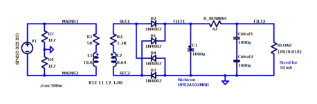
At start up, the two 1000uF capacitor in series are at 0V.
Their voltage rise time is determined by the RC of 47R/500uF.
It is easy enough to simulate in Spice the transient current through the 47R, which will be 1.7A peak.
Yes, it will last very briefly.
But the datasheet also allows something like 1us.
I would certainly use a slow ramp in the power supply which has a larger time constant.
But as long as you are happy, all is fine.
Patrick
It is easy enough to simulate in Spice the transient current through the 47R, which will be 1.7A peak
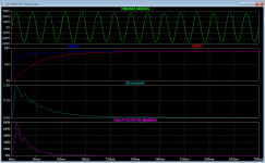
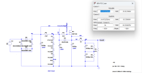
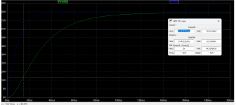
I did, schematic attached below. The transient current through the 47R was 1.3 amperes peak (cyan trace, 3rd panel), and the peak instantaneous power dissipation in the 47R resistor was 80 watts (purple trace, 4th panel). Instantaneous power dissipation decayed to "normal" after about 70 milliseconds.
_
Attachments
Thank you Patrick for pointing out the power dissipation issue. I am always learning on my diy journey so it is always appreciated.
Thank you Mark for the simulation.
I also simulated the power up, but with the power supply (a zener shunt regulated mosfet voltage follower with 1000uf capacitor at DC input and DC output) included. The maximum voltage drop across the 47 Ohm resistor was 45V, so approximately 1A, My simulation was not as sophisticated as Mark's simulation as I did not include the power transformer (I am not at Mark's level of electronics knowledge, nor at Patrick's level either). 😊
By the way, I had problems finding a transformer with the correct secondary voltage so that is why the preregulated voltage is so low. Higher input voltage would have been better but I used what I had.
I will upgrade the resistor to a higher Wattage in the future just to avoid any failure, but it is surviving in the short term.
Attachments
It's in the style of Nelson's DIY FE 2022. It may be powered by a non-regulated supply, a SMPS, or other power supply. The RC on the board offers a bit more filtering.
The extra capacitors on the board also allow flexibility in the use of V+, V-, or bipolar power supply.
I unashamedly copied Nelson's design. 🙂
The extra capacitors on the board also allow flexibility in the use of V+, V-, or bipolar power supply.
I unashamedly copied Nelson's design. 🙂
Here is a picture of the power supply and the new right channel installed. The DIY FE 2022 was still in the left channel location.

The power transformers are Hammond 187B36, centre tapped, rated at 36V @ 0.17A. There are two of them with the secondary windings connected in series, and output using 3/4 of the secondary windings (54VAC). Finding the right transformer(s) was difficult. It seemed that lately the variety of electronics components available for purchase is much less and prices are much higher.
From an voltage selection point of view, I have found it difficult to predict the secondary voltage under low load for low current demand from low VA transformers, and it was no exception in this case. Luckily the transformers are centre tapped so I was able to use the centre tap on one of the transformers in order to keep the DC voltage under 100V.
Below are the distortion plots for the right channel with 80VDC power. The maximum output voltage was nearly 19Vrms. Gain was 10X. The maximum output voltage was limited by the maximum voltage output of my 1kHz oscillator. I will be changing the gain to 16X. That would suit my system best as my digital source is a TDA1541A DAC with only an I/V resistor and no electronic gain.
According to the datasheet in post #9, the PR01, which is 1W and correct size to suit the current PCB footprint, can survive 80W repeatedly for 0.02ms.Instantaneous power dissipation decayed to "normal" after about 70 milliseconds.
Going to PR03 (3W) will improve it to ~2ms.
This will of course improve further when using split rails, with 1x47R for each rail.
Patrick
FFT plots for 80VDC power supply and 16X gain. Maximum output voltage was attained: 27Vrms = 38Vp. Distortion was higher with the higher gain, which was expected. It is still low enough for me. 🤓


Always fun to read your posts Ben. I have a general idea of what the OP amp is doing, or I think I do…
With my inability to nerd out on electronics design, besides the ability to provide full voltage swing for the followers, was there any other “design goals” ?
I assume part of it is fun, and having decent levels of distortion. Both good things around these circles.
I am curious if you plan on tweaking parameters on the Front end affects the followers/ performance overall.
I am a self taught electronics diyer, I am constantly learning, and this project is another learning experience. I try to do something different in each of the projects that I take on. So that is my goal.
.
It's all for fun, with no hard and fast performance expectations, although there is a lot of hope.
It is all part of the hobby, coming up with an idea, LTspice simulations, pcb design, build, testing, trouble shooting - all brain exercise. For me it is the process that I enjoy. And it's great that I end up with equipment that plays good sounding music! 🤓
- Home
- Amplifiers
- Pass Labs
- A Higher Voltage DIY Discrete Op Amp - In the Style of the DIY FE 2022