Well, I have designed and made a 4kW full-bridge SMPS with SG3525, with voltage control - no current control yet. Before you jump on me, remind that this is my very first SMPS project, so I am not that skilled in this stuff.
The DC output is 2x60V and it is pretty nice regulated. I use this supply to feed two 1500W tripath bridged amp modules.
And my problem is. After power-up, everything works fine. No EMI or RFI propagation. But, after a minute or so, the supply starts to produce VERY nasty and strong hi-frequency EMI into mains.
I am only using 1uF capacitors at mains - in front of the bridge and second 1uF is after the bridge.
I think it is easiest to say that I have to get some more EMI filtration on mains. Definitely I am going to. But why the noise is not propagating the first minute after power-up? I though it has sometning to do with the temperature, but it does not. Because when that EMI starts propagating and I shut the supply down even only for a second or so, it still takes about a minute to start interfering.
I think this may have something to do with transformer's saturation. Because there is a full-bridge switching, the transformer can easily come into saturation when switches are not symmetrical. I have read that this can be solved with a capacitor, connected in series with the primary winding, but I do not know the required capacitance for my supply.
Could somebody please help me and tell me if this EMI problem is caused by the transformer saturation or maybe something else?
P.S. the supply is behaving very good at normal cirstumcanses, the tripath modules hooked on have driven two 1000W woofers a lots of times before... but there is still that problem with EMI.
Hmm weird! I don't know anything about EMI, so I'll stick to the transformer: a capacitor with value say 10x greater than the impedance at that point will suffice. I.e. impedance = 10 ohms, 1 ohm or less reactance at 100kHz = 1.6uF... maybe a bit more for safe keeping. Hmm, that's about the value in domestic computer SMPS's of a tenth the rating, yet 10 ohms on +350V would give something over 10kW (very ballparkly). Sigh, thus ends my reign of rough, ohmic estimations... 🙁
Tim
Tim
Filter Cap
Dis-
Did you say the filter cap AFTER the bridge was 1uf? Are you PFC'ing the front end? If not, then your input cap (after the diode bridge) should be alot bigger than 1uF. Say, like 4700uf at 400V. (I assume you're powering this off the European 240V mains, yielding something like 330VDC after rectification, right?) I have made 12V push-pull switchers for car amps using the SG3525 in the past and have experienced the same EMI/RFI problem. I experimented by removing the feedback optoisolator and letting the circuit run full wide-open at max duty cycle. As expected, the outputs rose to +/- 56V (they were regulated to +/-37V), but the noise disappeared. Hmmmm... 😕
Anyhow. I fiddled with the output filtering (the original schematic had only a capacitor) by putting a series inductor after the output rectifier, but before the main output filter caps. I wanted to wind both (+) and (-) outputs bi-filar on the same core for perfect cancellation, but the pc board layout was not set up for it. Nevertheless, the inductors got rid of most of the noise.
I further modified the design by implementing current-mode control using Unitrode (now Texas instruments) UC1846, and LCLC outout filtering. Not a whisper of noise anywhere on the spectrum. The schematic for the '1846-based supply was provided to me by Mr. Randy Vikan, the author of an article in Audio Amateur 1989/90 about his 75W/ch MOSFET car amp.
Don't worry about the SG3525, we won't beat you up too much! 😉 .
Nowadays, I prefer to use ONsemi's MC33025. This chip is a close cousin of the SG3525 (nearly the same pinout), and can be run either voltage- or current-mode. It has high-current totem-pole outputs (+/-2A) to drive transforemers or MOSFETs directly.
OK, regarding the coupling capacitor in series with the main transformer, you will definitely need one with voltage-mode control. It is optional with current-mode, because of c-m's pulse-by-pulse current limiting feature. This corrects for almost any MOSFET imbalance that there night be.
Getting back to the formula for the coupling capacitor, here it is:
Cc = [I(max) * dT] / dVCc
Where Cc is the coupling cap (in uF), and dVCc is the max voltage ripple across the coupling cap (set this at 30V) and dT is 1/F(sw) (16.67uS for F = 60kHz).
We get I(max) by taking I(d) *1.2 = I(max), where I(d) is the max drain current of the MOSFETs.
I(d) = [1.56 * P(out)] / V(in(min)), where Vin (min) is 180VAC, or 254VDC.
So, I(max) = (1.56 * 4000) / 254V = 24.47A
Now we can find Cc.
Cc = (24.47 * 16.67 e-6) / 30 = 13.59uF for your coupling cap. For safety's sake, make this 15uF by paralleling 15 - 1uF non-polarized caps, and rate them for 400Vdc. 600Vdc would be even better.
Sch3mat1c, do you concur?
Best of Luck, and please post pics and results.
'73,
de N8XO, Steve 😀
I have built a similar supply with the same chip (SG3525) in full bridge topology and had an audible noise coming from the transformer. I looked at everything- there was this persistent noisy (audible and electrically) operation, mostly with no load. I could see the primary current waveform saturating on certain pulses. Pulse width was choppy, etc. I added a 560pF cap from the COMP pin to GND right on the SG3525 and it cleaned the supply up dramatically. Additionally, I somehow did not need a cap in the primary as is suggested. My tranfo was made split secondary (S-P-S) with copper foil windings. It operated just fine with no saturation that I could tell after that simple cap addition
Just a thought!
Matt.
Just a thought!
Matt.
Hmmm.... That is interesting. Playing with the feedback compensation loop cleaned it right up?
I do have cut-n-dried procedure for calculating ther R-C components of the feedback loop (several procedures, actually). I cobbled them together from Chryssis', Pressman's and Brown's books.
The main differences between the methods are driven by the topology and control method (fly-back -v- forward, PWM -v- resonant/quasi-resonant). Perhaps I was using the wrong procedure.
I will go back and re-examine things. I did leave extra psaces on the pc board layout to accomodate different compensation schemes.
N-Channel,
I suppose there was some high-freq noise getting into the output of the on-board error amp in my case. The COMP pin is a pretty critical pin- not as much as the clock, but the noise into the PWM was causing the pulses to jitter enough to cause audible noise from the supply. If you look at the SG3525 data sheet, they include a cap in this location on thier sample/test circuit as well. IMO, this is independent of the feedback compensation components and it would just have the effect of slowing the entire response a bit. Your other calculations, I would think, would remain the same.
Off topic, but I'd like to see your calcs for R-C components as it relates to audio circuits (if they differ from a regular supply). I had some unresoved problems with a low freq. resonance with the same voltage mode controlled circuit. I was thinking that it was from the L-C on the output on the supply. I was using the supply to drive a classic class AB amp, and with a 200Hz sine wave into the amplifier, the primary current on the supply had these nasty peaks with about a 400Hz envelope that was audible on the output on the amp. Everything cleared up at higher and lower frequency audio signals. I adjusted to compensation components and the L and C and it would just shift the resonance around. I was using the pole-zero comensation from Brown's book, but there are quite a few errors in it. Not sure if I missed a pole, or something. I've read as much as I could on compensation loops, and I still don't seem to have a grasp of them very well. Oh well, I guess topic for another discussion.
Loopy!
Compensation loops are indeed a tricky thing! I had to dig to get the calculations for the Coupling cap, but the calcualtions for the RC compensation components are mostly from Brown's book. I think Brown does mention that compensation can be either on the primary or secondary side (if isolated). I think the half-bridge ckt based on the MC33025 used secondary-side compensation at the TL431, and disabled the MC33025's on-board error amp.
Compensation loops are indeed a tricky thing! I had to dig to get the calculations for the Coupling cap, but the calcualtions for the RC compensation components are mostly from Brown's book. I think Brown does mention that compensation can be either on the primary or secondary side (if isolated). I think the half-bridge ckt based on the MC33025 used secondary-side compensation at the TL431, and disabled the MC33025's on-board error amp.
Try a 22pf cap to ground from the osc. out pin 4. On the similar 1825 pwm chip (called the clock pin on this i.c.) this can work miracles for noise and stability problems that develop after a minute or two of being powered. I've seen this problem on many occasions on several types of current mode SMPS and 22pf is optimum with the 1825 every time. The only voltage mode one that had the problem needed a higher value, 220pf if I remember correctly.
First of all, I am very glad there is this much interest in my problem. Thank you all, guys.
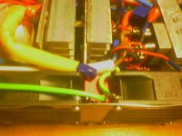
Originally I have got two 100uH, but really BIG inductors for both positive and negative rail separately, followed by 3x330uF/100V Panasonic EB series caps per rail. The filter is made better than calculated (originally 60uH and 30uF would suffice for 10% current ripple at full load)
I am attaching a photo of this.
As entire control circuit is on the secondary side (I drive the MOSFET gates through pulse transformers), there is no optocoupler in the feedback loop. Just a zener diode and a voltage divider to set the desired voltage.
The third modification made now was putting a 100pF/1kW cap and 100R/2W in series paralelly to main transformer's primary winding. Previously, I had them there for evaluation, but I removed them... don't remember the reason. But now I put them back because I think it may help reducing EMI.
NOW THE RESULT:
-Really significant reduction of EMI into mains, input and output cables and into ether (now I can put the mixing console right on the amp and there is no audible hiss or noise anymore). Anyway, there is still significant interference with VHF mics at the events, I can even see both diversity A-B leds bounce to the bass I would really like to fix this, because now I have to increase the squelch setting of the VHF receiver and this decreases the mic's maximum working range.
-Better voltage stability (before, the LEDs connected thru resistors to + and - rail against ground were visibly showing the voltage fall at full-power bass peaks. Now, the light has significantly more constant intensity, telling me that voltages are more stable.
-Better start-up sequence and small load operation(before, there were large VPP and VNN oscillations of about 2-3Hz and 30V amplitude, that caused the chips in both amplifiers go into undervoltage protection with only 1mA current draw. I had to toggle the power switch several times and if lucky, it started up 🙂
Now, I can only see a voltage drop right after the amps get from UV protection to normal operation mode, but I think this may be caused with large supply soft-start capacitor (47uF), who causes the PWM duty cycle, and supply voltage respectively to raise slowly.
I am sorry for the quality of attached photo, but it is taken only with mobile phone's cam. I do not have a digital camera.
No, of course primary filtration is much more than 1uF. There are four paralelled 1000uF/400V EPCOS low ESR caps. That 1uF caps before and after mains bridge rectifier are mainly for RF filtering.Did you say the filter cap AFTER the bridge was 1uf? Are you PFC'ing the front end? If not, then your input cap (after the diode bridge) should be alot bigger than 1uF. Say, like 4700uf at 400V. (I assume you're powering this off the European 240V mains, yielding something like 330VDC after rectification, right?)
I have not heard of winding opposite currents' wires onto one core. Do I have to wind them parallel, or opposite direction?Anyhow. I fiddled with the output filtering (the original schematic had only a capacitor) by putting a series inductor after the output rectifier, but before the main output filter caps. I wanted to wind both (+) and (-) outputs bi-filar on the same core for perfect cancellation, but the pc board layout was not set up for it. Nevertheless, the inductors got rid of most of the noise.
Originally I have got two 100uH, but really BIG inductors for both positive and negative rail separately, followed by 3x330uF/100V Panasonic EB series caps per rail. The filter is made better than calculated (originally 60uH and 30uF would suffice for 10% current ripple at full load)
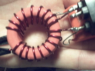
According to this, I calculated the capacitance at 250kHz would be 3,33uF. So I bought five 680uF/400V WIMA quality foil caps, glued them together, paralelled them, glued onto chassis between fans 🙄 because there really wasn't room on the PCB, and the closest place to the transformer was right between the fans. 🙁OK, regarding the coupling capacitor in series with the main transformer, you will definitely need one with voltage-mode control. It is optional with current-mode, because of c-m's pulse-by-pulse current limiting feature. This corrects for almost any MOSFET imbalance that there night be.
I am attaching a photo of this.
I did this too. Originally, the compensation loop was like 470k resistor in parallel with 68nF cap connected between INV IN and COMP pins, and a 10nF cap from COMP to ground. So I removed that resistor and cap and replaced them with one 10k resistor, as shown on schematic in SG3525's datasheet.I added a 560pF cap from the COMP pin to GND right on the SG3525 and it cleaned the supply up dramatically.
As entire control circuit is on the secondary side (I drive the MOSFET gates through pulse transformers), there is no optocoupler in the feedback loop. Just a zener diode and a voltage divider to set the desired voltage.
The third modification made now was putting a 100pF/1kW cap and 100R/2W in series paralelly to main transformer's primary winding. Previously, I had them there for evaluation, but I removed them... don't remember the reason. But now I put them back because I think it may help reducing EMI.
Unfortunately, I have read this post just after I have completely mounted the device into the chassis, so I did not made this modification yet. But it sounds good, I will definitely put that cap in a bit later.Try a 22pf cap to ground from the osc. out pin 4. On the similar 1825 pwm chip (called the clock pin on this i.c.) this can work miracles for noise and stability problems that develop after a minute or two of being powered.
NOW THE RESULT:
-Really significant reduction of EMI into mains, input and output cables and into ether (now I can put the mixing console right on the amp and there is no audible hiss or noise anymore). Anyway, there is still significant interference with VHF mics at the events, I can even see both diversity A-B leds bounce to the bass
I would really like to fix this, because now I have to increase the squelch setting of the VHF receiver and this decreases the mic's maximum working range.-Better voltage stability (before, the LEDs connected thru resistors to + and - rail against ground were visibly showing the voltage fall at full-power bass peaks. Now, the light has significantly more constant intensity, telling me that voltages are more stable.
-Better start-up sequence and small load operation(before, there were large VPP and VNN oscillations of about 2-3Hz and 30V amplitude, that caused the chips in both amplifiers go into undervoltage protection with only 1mA current draw. I had to toggle the power switch several times and if lucky, it started up 🙂
Now, I can only see a voltage drop right after the amps get from UV protection to normal operation mode, but I think this may be caused with large supply soft-start capacitor (47uF), who causes the PWM duty cycle, and supply voltage respectively to raise slowly.
I am sorry for the quality of attached photo, but it is taken only with mobile phone's cam. I do not have a digital camera.
Attachments
pics
Here are some more
http://www.anonym555.kgb.cz/amp.rar
You can see the final look of the amplifier, its inside, and a SMPS schematic (this is not very accurate now, there is other kind of PFC-PWM synchronisation and there are these three modifications I mentoined). I also attached a photo of a burned 18Sound 1000W AES bass speaker, just for fun 🙂
That is caused by that class-T switching beasts. Maybe I did something wrong, maybe their algoritm is bad... who knows. But speaker's diaphragm was not damaged, so most likely there are some nasty DC peaks or something...
Such a SMPS must not be left unfiltered. A common mode filter should be placed at the mains input. In order to build the required common mode choke just wrap two symmetrical windings across a high permeability ferrite toroid. Use as many turns as possible. See the picture for more details:
What an impressive SMPS, Disney_SK!
Are you willing to share the schematics with us? I am also in my way of building a half-bridge SMPS, somewhat smaller, however (around 800W).
I also use a SG3525, but it's in the primary side because I use mains + hv regulator for startup, so I really need an optocoupler. However, I am experiencing basic problems with voltage mode control, so having a peek at your controller (feedback, decoupling, compensation...) could help me a lot.
Also, what power devices are you using, IGBT's or Mosfets? Eva has provided some very good advices to me about that and now I am not completely sure about my first approach: mosfets ;-)
Thanks in advance!
I totally agree with Mr. Eva... you can't connect such a monster directly to mains without any kind of filter.
For a quick and dirty solution, you can try to take a pair of yellow toroid (from a normal PC psu) and give some turns of copper (at least 2mm diam., then with a scope measure the noise, and try to oppose the fases.
Hope you'll be able to understan what I mean.... my english is so bad
For a quick and dirty solution, you can try to take a pair of yellow toroid (from a normal PC psu) and give some turns of copper (at least 2mm diam., then with a scope measure the noise, and try to oppose the fases.
Hope you'll be able to understan what I mean.... my english is so bad
Pierre said:What an impressive SMPS, Disney_SK!
Are you willing to share the schematics with us? I am also in my way of building a half-bridge SMPS, somewhat smaller, however (around 800W).
I also use a SG3525, but it's in the primary side because I use mains + hv regulator for startup, so I really need an optocoupler. However, I am experiencing basic problems with voltage mode control, so having a peek at your controller (feedback, decoupling, compensation...) could help me a lot.
Also, what power devices are you using, IGBT's or Mosfets? Eva has provided some very good advices to me about that and now I am not completely sure about my first approach: mosfets ;-)
Thanks in advance!
Of course I can provide the schematics, I already did... but as I see that server has some problems, so I will try to provide the content at http://www.djsonic.sk/amp.rar
I am currently using MOSFETs, but maybe I will move to IGBTs because of their capability to withstand longer current peaks... they do not explode so nasty as mosfets ;-)
rinox said:I totally agree with Mr. Eva... you can't connect such a monster directly to mains without any kind of filter.
For a quick and dirty solution, you can try to take a pair of yellow toroid (from a normal PC psu) and give some turns of copper (at least 2mm diam., then with a scope measure the noise, and try to oppose the fases.
Hope you'll be able to understan what I mean.... my english is so bad
I understand. EPCOS 10A off-the-shelf mains filter came few days ago and looks forward to be mounted in 🙂
I have just been having a look at your schematics...
Do they reflect the changes you have done to the control circuitry so it is estable? I don't think so, because it doesn't show the 560pF from COMP to GND, nor the suggested 22pF from OSC_OUT to GND but it shows the original values you said.
Did you finally include the modifications in your prototype and, if so, did they improve something?
It doesn't show the snubber, as well. Did you measure the primary waveform before and after putting it? Did that waveform improve or did you added it "just in case"?
Best regards,
Pierre
Pierre said:I have just been having a look at your schematics...
Do they reflect the changes you have done to the control circuitry so it is estable? I don't think so, because it doesn't show the 560pF from COMP to GND, nor the suggested 22pF from OSC_OUT to GND but it shows the original values you said.
Did you finally include the modifications in your prototype and, if so, did they improve something?
It doesn't show the snubber, as well. Did you measure the primary waveform before and after putting it? Did that waveform improve or did you added it "just in case"?
Best regards,
Pierre
You're right, this is the original schematic. I have no schematic but I did the changes discussed.
Added snubber consists of 100R/2W resistor and 100pF capacitor. I did not ever measure primary waveforms (too high voltage for me
 )
)I did not add that 22pF to OSC_OUT, but I have made other modifications which I have explained in another topic
(sorry but i don't remember them right now
 but they were made in accordance to http://www.djsonic.sk/car_supply.gif)
Following your post, you have replaced the resistor from INV_IN to COMP and now it is 10k, with no capacitor in parallel, and you have also added 10nF from COMP to GND. That's all?
But that doesn't match with the schematics of the 12V supply you have posted, right?
Sorry, I only want to have the point clear to start experimenting.
But that doesn't match with the schematics of the 12V supply you have posted, right?
Sorry, I only want to have the point clear to start experimenting.
Pierre said:Following your post, you have replaced the resistor from INV_IN to COMP and now it is 10k, with no capacitor in parallel, and you have also added 10nF from COMP to GND. That's all?
But that doesn't match with the schematics of the 12V supply you have posted, right?
Sorry, I only want to have the point clear to start experimenting.
Well, I have unmounted the control PCB and chcecked it especially for you 😉
now I don't remember which pin is "comp" and so on, so>
560pF and 10nF in parallel from pin at the edge to ground
10k resistor from pin at the edge to the one next to it.
I know this specification is a bit weird... but you know, summertime... people have other interests than smps 😉
- Status
- Not open for further replies.
- Home
- Amplifiers
- Power Supplies
- 4kW SMPS RFI problem