Why bother with a single sided PCB, double sided ones are just as easy to make at home if you are using either the toner transfer method or the photo method. Just line up your art work while looking through it, tape it together so it wont move, then insert your PCB.....Unless of course you have a stack os single sided boards you need to use up😀
The real question is this: Why bother aligning the two sides when it is not required due to the simplicity of the circuit?
It's all preference man, it is easier to make single sided and if that is what he likes he can have it that way...and you can have double sided! 🙂
I'll take 4-layer please...LOL 😀
-Matt
It's all preference man, it is easier to make single sided and if that is what he likes he can have it that way...and you can have double sided! 🙂
I'll take 4-layer please...LOL 😀
-Matt
zagisrule! said:The real question is this: Why bother aligning the two sides when it is not required due to the simplicity of the circuit?
It's all preference man, it is easier to make single sided and if that is what he likes he can have it that way...and you can have double sided! 🙂
I'll take 4-layer please...LOL 😀
-Matt
Oh believe me I'm not knocking a single layer design, merely making a suggestion. The chipamp.com design is a good two layer one that's proven. I've seen a few other single layer designs for this chip floating around, but most are larger and have long narrow traces. If a single layer design works for you by all means go for it
😀
On the initial schematic:
Power traces seem thin as they work through the chip.
Some of the other traces look like the output to PDF screwed them up some? Either that or the lines don't line up well (for example, follow the ground to pin 19).
I think the nature of this chip simply does not lend itself as well to a single sided board. IMHO a pair of 3886's would make more sense if single sided is the goal.
And... tiny traces on double sided? What?!
1.5"x2" - expects a large cap PSU of some sort.
Paralleled.
C
cjd wrote...
Power traces are thin... taken
the path to pin 19 is thin and will rectify it. I just converted the Word file (used Wordart on MAC) for posting and will not use it for making the PCB.
True. 4780 is difficult compared to 3886, but when a friend gets 4 free samples and gives u 2, u know...
Gcollier
I would love to go double sided but getting a single sided cclad glass epoxy itself is a nightmare ...and My India is a big country and volume orders are only entertained.
Besides IMO, the single sided is easy to rework on.
I have decided to fix hollow rivetts for the IC pins for reliability and long solder joint life, if I get the right size.
Gajanan Phadte
ThanksSome of the other traces look like the output to PDF screwed them up some? Either that or the lines don't line up well (for example, follow the ground to pin 19).
I think the nature of this chip simply does not lend itself as well to a single sided board. IMHO a pair of 3886's would make more sense if single sided is the goal.
Power traces are thin... taken
the path to pin 19 is thin and will rectify it. I just converted the Word file (used Wordart on MAC) for posting and will not use it for making the PCB.
True. 4780 is difficult compared to 3886, but when a friend gets 4 free samples and gives u 2, u know...
Gcollier
I would love to go double sided but getting a single sided cclad glass epoxy itself is a nightmare ...and My India is a big country and volume orders are only entertained.
Besides IMO, the single sided is easy to rework on.
I have decided to fix hollow rivetts for the IC pins for reliability and long solder joint life, if I get the right size.
Gajanan Phadte
gmphadte said:cjd wrote...
Thanks
Power traces are thin... taken
the path to pin 19 is thin and will rectify it. I just converted the Word file (used Wordart on MAC) for posting and will not use it for making the PCB.
True. 4780 is difficult compared to 3886, but when a friend gets 4 free samples and gives u 2, u know...
Gcollier
I would love to go double sided but getting a single sided cclad glass epoxy itself is a nightmare ...and My India is a big country and volume orders are only entertained.
Besides IMO, the single sided is easy to rework on.
I have decided to fix hollow rivetts for the IC pins for reliability and long solder joint life, if I get the right size.
Gajanan Phadte
How about 2 single sided boards stacked one on top of another 😀
LOL!
Gcollier said:
How about 2 single sided boards stacked one on top of another 😀
LOL!
A most excellent idea IMHO! 🙂 A bit thick perhaps. But only V+ and V- on the "bottom" is needed, and things clean up quite nicely! I put a couple other traces on the bottom of mine since it was there, but they need not be.
The other thing is it may be worth (carefully!) re-bending the pins so the power traces can be made thick and straight - alter the footprint of the chip.
Or bend them out so they're not attached to the PCB at all and run a solid copper wire for each (partial P2P basically).
C
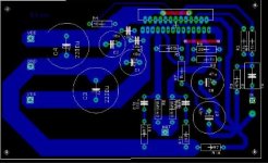
Componenet Layout
I have to first write that this is not my effort, only that i modified it a little.
The component layout is for parallel circuit. Just added input R andC for stereo use.
Gcollier wrote
Too good an idea IMO. Thanks. Never thought of it but is different thinking.
Upupa Epops wrote...
Nice quote, but if a guy has only one hand...
Gajanan Phadte
I have to first write that this is not my effort, only that i modified it a little.
can u post the component layout for the pcb that is given .....
The component layout is for parallel circuit. Just added input R andC for stereo use.
Gcollier wrote
How about 2 single sided boards stacked one on top of another
Too good an idea IMO. Thanks. Never thought of it but is different thinking.
Upupa Epops wrote...
It's like cratch left ear by right hand. Leave your amateur thinking .
Nice quote, but if a guy has only one hand...
Gajanan Phadte
Attachments
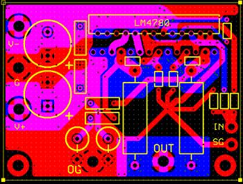
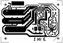
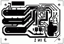
Corrected ?...
Here is a better pic...
For those of u with Qs
There are 3 jumpers to be installed
The small copper tracks indicate their location e.g. at pin 10 to 18,...
It is for stereo without modification. Connect speakers to IC output pins without the 2 resistors.
Provision for mute switch.
trouble due to layout to pin 9
Just cut 8-9 track and install jumper between diamonds from 9
Any commentts(+/-) are welcome.
Gajanan Phadte
Attachments
For newbies...
Just to give complete info
Component side view
Black number=Resistor, Purple number=Capacitor, orange is jumper.
4780 parts list
Self PCB Value Resistor code for 1% MFR
Last color (Brown) is tolerance
R1,R2 1K Brown, Black, Black , Brown
R3,R4 15K Brown, Green, Black, Red
R5,R6 20K Red, Black, Black, Red
R7,R8 1K Brown, Black, Black , Brown
R9.R10 0.1/3W
R11,R12 2.7
R13 10K Brown, Black, Black, Red
R14 2.7 (*not shown on schematics)
C1,C2 0.1
C3,C4 10 Watch polarity
C5,C6 1000 Watch polarity
C7,C8 47(68) Watch polarity
C9,C9 1 Watch polarity
C10,C11 0.1
Remember when u make the pcb, the copper side should look mirror image of the above.
First have the 4780 datasheet pdf from www.national.com
Now look at the picture of the IC on page 2 and look at the IC. Now locate pin 1 on the IC and on the board, on the component side(the side that has no copper) on a single sidded board. This is a single sided board, isn’t it.
Select which circuit u want to make, fig.3 or fig.7
easiest to make is fig7 as pcb does not require additions. R9, R10 are not installed for this.
Follow polarity for Capacitors from the schematic diagram.
There are 2 positions possible for resistor 13, One is for Mute switch as shown in schem.
Install only one resistor wherever needed
Attachments
Best...Idea...Ever!
 BEST IDEA EVER!!!!!!
Once I save up moolah to get the DGX Prototyper, no more having to use double sided boards and having to plate them (in the future of ever needing to! (when I get that mill!!!!!))😀 😀 😀 😀
Gcollier said:
How about 2 single sided boards stacked one on top of another 😀
LOL!
BEST IDEA EVER!!!!!! Once I save up moolah to get the DGX Prototyper, no more having to use double sided boards and having to plate them (in the future of ever needing to! (when I get that mill!!!!!))😀 😀 😀 😀
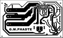
The star is imported from national pcb design.
U are shorting the provision for bridge config. The thin track and a incomplete track is a changeover arrangement. Cut one and connect another for bridge config
Gajanan
U are shorting the provision for bridge config. The thin track and a incomplete track is a changeover arrangement. Cut one and connect another for bridge config
Gajanan
gmphadte said:The star is imported from national pcb design.
You are shorting the provision for bridge config...
Ah, I wonder why a star, seems like a waste of good copper 🙂
And yes, I was being quick and dirty - just trying to illustrate the idea.
I would go for a solder-bridge, rather than cutting a track. Just my preference. 🙂
The star is like lanes rather than a crowded ground (like football)
Lot of thinking has gone into this pcb design. Remember, it is a stereo ready design and only needs changes if u want to make other configs i.e. parallel or bridged. So do not try to modify it unless u are very sure.
Enjoy
Gajanan Phadte
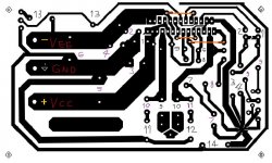
No cuts and bridges needed for stereo application. However there are 4 compulsory jumpers.I would go for a solder-bridge, rather than cutting a track. Just my preference.
Lot of thinking has gone into this pcb design. Remember, it is a stereo ready design and only needs changes if u want to make other configs i.e. parallel or bridged. So do not try to modify it unless u are very sure.
Enjoy
Gajanan Phadte
- Status
- Not open for further replies.
- Home
- Amplifiers
- Chip Amps
- 4780 single sided pcb redesigned