Mooly you are completely correct, I am not sure any longer.🙂
My first thought was to make two turn buttons, one on each side, left most a balance control and right most the volume control, in between these an 4 button input selector. That would look neat and would be a nice interface.
But the do the reality struck, that an input selector maybe will be a complicated project, when a simple 4 step turn button can do the same and maybe even a lot better and reliable.
I am not interested in making the volume control as a two button solution, then are there only the balance control left. And did I think, this could maybe be solved fairly easy-ish.
And, as you say, the balance is not something I do need often but is fairly nice when a recording is slightly skewed toward one side.
I have chosen to use solid state relays, just to keep it reliable and "noise free".
In short do everything sound as a great idea, until you ask those who in fact know what it's about (all you in here)!
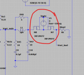
I am planning on using TLP3543AF
https://toshiba.semicon-storage.com/info/docget.jsp?did=60317&prodName=TLP3543A
https://toshiba.semicon-storage.com/info/docget.jsp?did=60317&prodName=TLP3543A
Hmm 🙂
Interesting devices. They are miniature versions of our discrete 'speaker relay' replacements that have become popular on the forum.
Erm... Now I'm not really sure these will be suitable tbh. Sorry, I don't like saying that when you had already chosen them but I'm wondering if the junction capacitance of the FET's will be an issue and allow audio to pass when off.
The problem is that power FET's always have a high capacitance between D and S, a few hundred to a thousand or more pico farads and that will pass the high frequency audio. Does that make sense?
Not any problem, just happy you save me that money and work on buying, soldering and failing🙂
Interesting about the capacitance, so that mean that any power-fet do have capacitance that is getting charged by the input signal? And caps do only block ac?
If I have understand correctly, should the above bee somewhat in the right direction🙂
Interesting about the capacitance, so that mean that any power-fet do have capacitance that is getting charged by the input signal? And caps do only block ac?
If I have understand correctly, should the above bee somewhat in the right direction🙂
Think of the FET itself as nearly 'perfect' so that it has very low on resistance (a good thing) and very high off resistance (also a good thing).
What spoils it is the unavoidable stray parasitic capacitance that appears across D and S.
So we have a perfect FET with a parallel capacitor across it.
That capacitor, although small in value will pass audio. The higher the frequency the more it passes.
For power applications and even our speaker relays it doesn't matter because the amount of audio is very small and the load impedance (the speaker) is very low. So you can't hear anything when its off... but a preamp switch is very different because it is working into high impedances and so the audio signal would be very obvious.
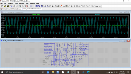
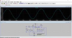
I even add these type of relays to simulations so you can see here the problem. I've made the speaker 6k so that the unwanted signal can be seen. The larger trace is the input and the small green one is the output. And this is supposed to be OFF.
What spoils it is the unavoidable stray parasitic capacitance that appears across D and S.
So we have a perfect FET with a parallel capacitor across it.
That capacitor, although small in value will pass audio. The higher the frequency the more it passes.
For power applications and even our speaker relays it doesn't matter because the amount of audio is very small and the load impedance (the speaker) is very low. So you can't hear anything when its off... but a preamp switch is very different because it is working into high impedances and so the audio signal would be very obvious.
I even add these type of relays to simulations so you can see here the problem. I've made the speaker 6k so that the unwanted signal can be seen. The larger trace is the input and the small green one is the output. And this is supposed to be OFF.
Attachments
Funny, I did chose that solution because of the two great features, not knowing about capacitance. It have an amazing low resistance.
Is there better solutions that you will recommend?
Is there better solutions that you will recommend?
One for tomorrow 🙂
but for preamp switching and working with higher impedances you don't really need the super low on resistance. I used individual little JFET's (which are totally different to the big power FET's in those relays).
There are two FET's per channel and per input. One FET is on and shunts the audio to ground on the non selected input/s and the other FET is OFF to block anything that might still be there.
For the selected input the switches reverse operation. You can add as many inputs as you want with this arrangement.
The results are pretty spectacular and there is absolutely no audible breakthrough even when applying really high level test signals.
Have a read around this post. Before and after.
I'm not saying you should use FET's, they need slightly difficult voltages for driving them but you could use in their place the cheap CMOS 4066 switches in place of the FET's.
Many will pull a face at that suggestion but the 4066 is great when used correctly in a circuit like this.
but for preamp switching and working with higher impedances you don't really need the super low on resistance. I used individual little JFET's (which are totally different to the big power FET's in those relays).
There are two FET's per channel and per input. One FET is on and shunts the audio to ground on the non selected input/s and the other FET is OFF to block anything that might still be there.
For the selected input the switches reverse operation. You can add as many inputs as you want with this arrangement.
The results are pretty spectacular and there is absolutely no audible breakthrough even when applying really high level test signals.
Have a read around this post. Before and after.
Hi,
O.K. The FET's as I use them give as near total isolation as is possible. With the volume of the amp on full and audio applied to all (3 in my case Aux, Mini Disc and tuner) unselected inputs there is no audible breakthrough at all. Even with 10 volts squarewave shoved up one of the inputs there is zero breakthrough even with ears right up to tweeter. None - nothing - - zilch 😉
Try those FET's you have.
I'm not saying you should use FET's, they need slightly difficult voltages for driving them but you could use in their place the cheap CMOS 4066 switches in place of the FET's.
Many will pull a face at that suggestion but the 4066 is great when used correctly in a circuit like this.
Attachments
My idea is to have least amount of components in the signal, I have managed to only have 2-3 components. My reason for choosing as low an impedance was to make the pre-amp look like a wire for the power-amp. I do just stumble around in the dark but it's fun, and when you are so great to advice me, I do happily listen! 🙂
What about if I added a normally closed fet, to lead the rest signal to ground?
What about if I added a normally closed fet, to lead the rest signal to ground?
This link:
FET Input Selector
shows the FET switching (circuit in post #28) in action. Notice at the end when I select the unused input and turn the volume up full. There is no audible breakthrough even though all three signal sources are active and playing.
The manual input selector knob also has full control over whatever input is selected and moving the knob to a new position generates a reset pulse and re-selects whichever new position the control is now pointing to.
The motorized control is an ALP's type.
"sounds" great🙂
Ill try to take a better look at it, to find out what is happening in that circuit.
Ill try to take a better look at it, to find out what is happening in that circuit.
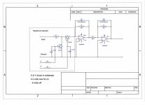
Everything in the rectangle that says 'repeat as required' is duplicated for each input you want. They all come together at the opamp inverting input but only one at a time is allowed through by the series FET.
The other FET shunts the unused input signal to ground.
The circuit works so well because the series FET sees essentially no voltage across it. Each FET actually has quite a high ON resistance, about 20 or 30 ohms at a guess but it doesn't matter.
The 18k input resistor determines the input impedance for that input and its value can be tweaked so that all inputs sound the same volume even the output level of the source components is different.
I'll let you do the maths 😉
So 18k in series with 30 ohms means most of the signal is shunted when the input is not selected. The open FET has a resistance of many hundred of meg ohms... and a parallel capacitance of just a few pico farads.
So nothing gets past 😉
The 4066 CMOS switches would easily stand in for the FET's and would be easier to interface to.
http://www.ti.com/lit/ds/symlink/cd4066b.pdf
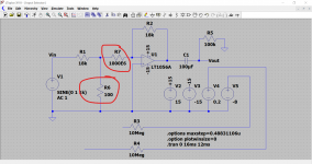
Mooly, sorry my late answer, but I thought it better to wait answering until I thought I have understood your schematic right.
As I sees it would the power never go past Q1 and Q2 if X and Y did not exists.
X and Y do not have any function after the rest of the circuit is activated?
C3 and C4 is a sort of delay to slow down the fet's reaction time?
After the K1 is supplied power do K1 reverse polarity to make the Q1 and Q2 keep working.
K2 is to make the polarity back to the original polarity.
The components across K1 and K2 is because you can't get enough power trough an op-amp.
The first 18k do I understand, as you explain it's function, but why an extra 18k between the op-amps?
To me does it look like that Q1's only function is to ensure to drag the fet's low, to activate them.
If the fet's were guaranteed to close at zero volt, would non of the op-amps be necessary?
The 4066 CMOS switches would easily stand in for the FET's and would be easier to interface to.
Nice video, Mooly. You mean use the 4066 in a T-Switch topology - like so?
https://www.electroschematics.com/multiplexer-switch-with-4066/
Not quite... the way I have it configured is to feed the selected audio into a virtual earth mixer circuit which means you see no (easily measurable) signal at the opamp input. My method uses one switch less per feed as well.
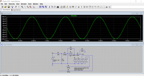
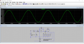
Lets see if I can show it. Here is the FET version in on and off mode. Look at the scale for the off state. We are applying 1 volt peak and getting around 38 nano volts peak coming out.
If we didn't use the virtual earth mixer then we would see both a significant signal voltage across the FET's and also the FET junction capacitance from D to S would be more dominant as it would be working into whatever load you attached rather than something that is essentially 'ground'.
Attachments
Mooly, sorry my late answer, but I thought it better to wait answering until I thought I have understood your schematic right.
As I sees it would the power never go past Q1 and Q2 if X and Y did not exists.
X and Y do not have any function after the rest of the circuit is activated?
C3 and C4 is a sort of delay to slow down the fet's reaction time?
After the K1 is supplied power do K1 reverse polarity to make the Q1 and Q2 keep working.
K2 is to make the polarity back to the original polarity.
The components across K1 and K2 is because you can't get enough power trough an op-amp.
The first 18k do I understand, as you explain it's function, but why an extra 18k between the op-amps?
To me does it look like that Q1's only function is to ensure to drag the fet's low, to activate them.
If the fet's were guaranteed to close at zero volt, would non of the op-amps be necessary?
X and Y are the two logic control signals. Like High and Low (1 and 0) but here High = 0.3 volt and low = -8 volt.
Taking the gate high (0.3 volt) turns the FET fully on. We could actually just take it to zero volts but that misses squeezing the FET down to the lowest possible on resistance.
So Q1 is ON when that selected channel is not wanted. It removes most of the audio by shorting it to ground.
When Q1 is ON, Q2 is OFF and that block the last small amount of audio.
When you reverse the logic Q1 is off (so the audio is not shorted to ground) and Q2 is ON and lets the audio pass through.
C3 and C4 do indeed just make the logic change slow and gradual so that the changeover is softer... as you could hear in the video.
The second opamp just restores the original phase although it is debateable whether absolute phase even matters... most can not tell a difference anyway.
Oh okay, so your virtual earth mixer, from it's name, is a way to take grounds from different places and then join them there and ehm "mix" them or "mute" them?
The significant higher voltage, if the virtual earth mixer wasn't there, is that due to you been able to (have forgotten the word) move the virtual earth mixer up or down some voltage,compared to true ground?
The significant higher voltage, if the virtual earth mixer wasn't there, is that due to you been able to (have forgotten the word) move the virtual earth mixer up or down some voltage,compared to true ground?
Glad, I can see I did interpreted the mosfet part correct, did just not explain it correctly🙂
What you in fact has is a sort of Normally open and normally closed switch, depended on you want audio or not?
And yes you have made a sort of short cross fade from channel to channel.
That should reduce or eliminate any pop from switching input.
And yes the last opamp do bring everything (audio) back to it's normal phase again.
Thanks for making the illustration, they show me a lot, in combination with your explanation! 🙂
A virtual earth mixer is really just an inverting opamp stage. The way it operates means that the inverting input (that you apply the signal to) never moves away from ground potential (to all practical purposes).
Look at the configuration and think about the standard equation for gain in that configuration.
The gain is -(Rf/Rin) so it is -(18k/18k) which is -1
The - sign denotes inversion of signal.
So we have 18k on the input and 18k as a feedback resistor. If we apply +1 volt to the input we can see that the output must go to a level of -1 volt.
This gives 'zero' volts on the inverting input... good eh 🙂
Lets say we made Rf 180k. The gain would now be -10 and so would see -10 volts at the output.
The opamp input still sees zero volts because the currents in the two resistor sum perfectly to zero at their junction.
To really understand the circuit you need to remember the golden rule of opamps using feedback... so remember this 🙂
The output of an opamp with feedback will do all it can to keep the voltage difference between the two inputs at zero volts.
Do you see how that works now. We have tied the non inverting input top ground and so it is at zero volts.
We apply 1 volt to the inverting input through an 18k
The output of the opamp now has to keep the difference in voltage between those inputs at zero and so it has to go to -1 volts to do that.
Last one for today 😉
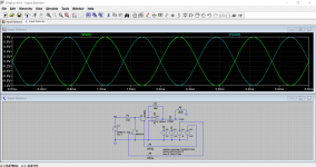
See if this makes sense. It is the same circuit but the FET's are replaced by resistances to make it easier to understand.
We will say that when on the FET has a resistance of 100 ohm and when off it has a resistance of 1000 megohm.
So when blocking the audio we get a level of 100 nano volts coming through (1V input).
Now lets do the same thing but this time we remove the opamp and feed the signal into the 100k load directly.
Look how much worse the OFF state is now. Much more gets through than if we used the virtual earth input stage.
Attachments
- Home
- Design & Build
- Construction Tips
- 4 btn Input selector, how?