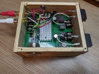
I just finished my very first amplifier, with schematics based on tpa3116d2 evaluation module (https://www.ti.com/lit/ug/slou336b/slou336b.pdf). The only change I made was to drop the gain to 20dB, and remove some jumpers. I threw together the box from 0.25" oak board pieces. All parts came from digikey, except the power button and connectors that I ordered on aliexpress. The PCB was designed in kicad and manufactured by jlcpcb. This was a very exciting project overall (for me). I still have a few remaining problems and would appreciate some help,
(1) The speakers emit some white noise when there is no input. It is barely audible, but becomes about twice as loud a few seconds after the input stops. Does anyone have an idea on what could be going on? In any case, I can still only hear it if I put my ear next to the speakers.
(2) I would like to have two stereo inputs in it. I was planning to add a mixer. Could someone please suggest a mixer that is decent and not too complicated to understand? I don't have enough experience in audio to design something like that. I did go over the mixer page (https://sound-au.com/articles/audio-mixing.htm) and some opamp theory in Sedra's book.
Thanks All.
Attachments
Last edited:
The long delay before the noise level gets larger implies a thermal sensitivity. It could be that it takes a few seconds for some small dc offsets in the error amplifier to reach a bias point where the two channels are synchronized by a lesser path other than the oscillator like a rising or a falling edge. The 2 channels talk to each other through their common points of Vcc and Ground. Also, they talk to each other because every high current trace is a transmitter and every circuit board trace is a receiver. I have known the noise level to double when 2 power oscillators that are on the same circuit board become synchronized.
I would move some of your input and output wires around while the amplifier is playing when the noise is the loudest to see if you can find a sensitivity there. Maybe the synchronization sensitivity is from your wiring. That is easy to try compared to re-doing a layout. Separating all the inputs from all the outputs is important when you are concerned about small effects.
Some switcher designs have high noise at their outputs but that is a design compromise because other designs have no perceivable noise on their outputs.
A good switcher layout requires short and fat as possible traces for power lines and it needs separation between power runs and small signal traces.
James361, thank you very much for the comment. Looking at my pcb, I did manage to route the fat power trace right under the chip amp, which could be a part of the problem.
I've cut the power trace that was going under the chip, and replaced it with a wire. It's interesting that there is still some noise, but it is nowhere near the level it used to have.
Looks like you have to study intensely the pcb-layout of the eva-kit for more improvement.
The traces carrying current are critical, even the magnetic stray field of output current can interfere with inputs.
Input loops should be as small as possible.
My latest TPA3118 pcb designs are based on 4-layer pcbs.
btw - there are few members here taking the challenge of such pcb designs from scratch.
You are welcome!😎

At the same time, it seems exaggerated....4 layer PCB for an old tpa.... 🤔Looks like you have to study intensely the pcb-layout of the eva-kit for more improvement.
The traces carrying current are critical, even the magnetic stray field of output current can interfere with inputs.
Input loops should be as small as possible.
My latest TPA3118 pcb designs are based on 4-layer pcbs.
btw - there are few members here taking the challenge of such pcb designs from scratch.
You are welcome!😎
You may consider it that way. But nowadays 4 layers are not expensive and this eases the power traces routing.At the same time, it seems exaggerated....4 layer PCB for an old tpa....
Admittedly this is a matter of "just because we can".
- Home
- Amplifiers
- Class D
- 3116D2 amp and some questions