Sorry, gannaji, my comments were in regard of the Apex quasi. And off thread. Too easy to get sidetracked sometimes.
Post #15 refers to the OP design.
Post #15 refers to the OP design.
irf530 , 9530 work great on an amp like this. replace all 4 bjt's with the two fets and set bias to 5.3 volts. it should be fast enough to not require the compensation capacitors either.
FWIW it will work as-is and do what the OP wants.
IF he already designed the PCB and already has the necessary parts, specially the power transformer, just go ahead, build and use it.
If all new parts have to be bought at regular price, specially the PT which is the most expensive component, then he might get a full kit instead, at least from a $$$$ and practicallity point of view.
Thank you all for your feedback.Every comment of yours is something new for me to learn.
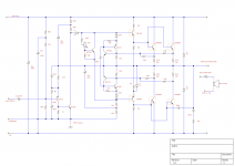
For this project I prefer to stay at this topology PNP input-NPN Vas and Quasi output and improve it to avoid potential problems you mentioned.It will be a low duty amp no more than 25 wattsat 8 ohm.
I will use either TIP41C or MJE15030 as outputs..I have built and listened the same schematic but with BD139-40 as drivers and 2SC5200 as output.I really liked the sound and is propably due to the harmonic profile it has.I have no scope to test square waves,clipping behavior,only LTspice.
Regarding the schematic i posted at the begining i would like to solve the problems you mentioned while retaining this topology PNP input-NPN Vas and Quasi output
.So far we have to
1. avoid output stage latch up
2. design for cleaner crossover distortion
3. fix temperature stability issues regarding the 2 feedback resistors 10k and 33k (changing the 10k resistor to something bigger would cure this problem?)
Anti-thump?
Anti-Thump circuit?
.So far we have to
1. avoid output stage latch up
2. design for cleaner crossover distortion
3. fix temperature stability issues regarding the 2 feedback resistors 10k and 33k (changing the 10k resistor to something bigger would cure this problem?)
Anti-Thump circuit?
Get the capacitor values correct and you won’t need an anti thump circuit. Just need some simulation and/or experimentation. And when you start getting thumps 20 years from now you know it’s time for a recap.
To answer your points in post #24:
1. This circuit does not suffer from latch-up in the way that the Apex retro does.
But it would still be a good idea to limit the VAS current with a small resistor in series with the emitter and a couple of diodes across the base to ground. To prevent the additional resistor from degrading the open loop gain the base resistor should be left connected between the base and emitter after including the emitter resistor i.e. not grounded. But the emitter resistor may help stability and transient distortion if you use the local feedback by keeping it grounded- this is a decision you might look into with a simulator.
2. Crossover distortion can be reduced - almost to the point of being as good as a fully complementary amplifier - if the Miller capacitor is connected between the output rail and base of the VAS. Sometimes this leads to oscillations which can be suppressed using a 220pF capacitor, or slightly larger, from the collector of the VAS to ground. This too has a downside in that it needs current to drive, and the VAS current may need to be increased as a result. Again this can be optimised in simulation.
3. The temperature effects will get worse with a bigger resistor. It needs to be smaller.
So my recommendation is to forget taking the feedback from the output capacitor. This was commonplace in the old days (and quite retro, so you may want to keep it) to reduce capacitor distortion, and possibly extend the bandwidth, but some contemporary designs gave excellent performance without needing this feedback. The bandwidth extension comes at a price of poor bass overloading - only a larger capacitor solves this.
If you swap the 10k for your 2.2k feedback resistor, (and don't need the 33k either) you solve the temperature drift issue. But you may have to readjust the input bias resistors to set the base of the PNP closer to mid-rail to get mid-voltage on the output rail.
mje15030 transistors are much faster then Tip41. if it is stable using those, the performance will be higher. This topology allows for very high bandwidth because of current feedback.
- Status
- Not open for further replies.
- Home
- Amplifiers
- Solid State
- 30Watt Quasi amplifier schematic