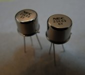
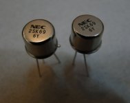
It has a TO-39 case, Vds of 140Volt at 100mA, 800mW dissipation with a Tj of 150C. VGs 7V max, GFS 30uS.
Hope that helps.
Hope that helps.
Difference between a Lateral MOSFET and a Vertical MOSFET is the orientation/position of the gate (+ oxide) layers.
It's a similar story for JFET's.
A regular JFET has the Gate as a parallel layer on top of the depletion zone, between Source and Drain areas on top of the substrate.
It's sorta built up as a wedding cake, in layers. (the build-up is symmetrical, the reason why Source and Drain of a JFET are interchangeable)
A VFET is actually a V-JFET, Vertical (trench) Junction (gate) FET.
The Gate area is buried, the build-up doesn't have a parallel (cake) structure, but with vertical areas. Hence the name Vertical, opposed to Lateral.
Lateral and Vertical MOSFETs behave somewhat differently, but operate in the same way.
Same story for JFET's and VFET's.
A K69 does a drain current of 100mA, so it's a Power JFET, but it handles 800mW max.
A regular N-channel JFET as e.g. K147 can do up to 30mA Idss, but handles 600mW.
In both cases, to test them, their dissipation should stay below the 800mW, respectively 600mW, otherwise it's all the same.
Means you should just read how to test a JFET, do a search, plenty measuring set-up sketches posted.
Last edited:
First of all, they are so much of a niche that I doubt it is a fake. Anyway, it should test as a jfet.
Second, on the curve tracer you should see a triode-like curves, that will confirm that is a V-fet.
Second, on the curve tracer you should see a triode-like curves, that will confirm that is a V-fet.
For a reference, he could check out a Sony K63, not exact same specs, but close enough for a VFET.
- Status
- Not open for further replies.
- Home
- Amplifiers
- Pass Labs
- 2SK69 datasheet?


