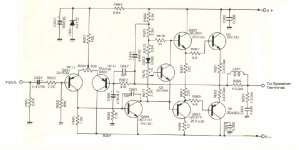
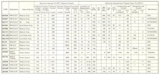
I have a 2x45W amplifier with a bad 2SA539 dc adjust transistor, TO-92 package. These are extinct, so I've attached the schematic and part specifications. The first 2 active devices are the 2SA539 and they are the first on the specs list.
Best that I ask for advice about a replacement. I’ve entered the specs into the Alltransistors search below and that might give some ideas, but I'm unsure which ones to avoid.🙂
Alltransistors.com Search for 2SA539
Best that I ask for advice about a replacement. I’ve entered the specs into the Alltransistors search below and that might give some ideas, but I'm unsure which ones to avoid.🙂
Alltransistors.com Search for 2SA539
Attachments
It's called the "long tailed pair" or differential amplifier pair. You need a fast, low noise PNP transistor with a Vceo at least as high as the supply voltage. That is not a difficult requirement. The original part is rated 60V and 200mA but here the current is 0.65/1k5 =~0.433mA so a 100mA part is fine. There are plenty of cheap Chinese parts that would work on Amazon by the dozen, but a better source would be Digikey or similar:
https://www.digikey.com/en/products/filter/transistors-bipolar-bjt-single/276?s=N4IgjCBcoGwJxVAYygMwIYBsDOBTANCAPZQDaIALGGABxwDsIAuoQA4AuUIAyuwE4BLAHYBzEAF9C9CohApIGHAWJkQAZho1aAJmZtOkHv2FjJIOruhy0WPIRKRyMOjEaEaVAAyeQhON5oYXxA4ChhaYLgAVjgwNWCwbzU4BEIwCk8oxISo+k9stJgKCij4tJptNVcEmiiKQODtOLU1H0JK5zq9EA4uXkFRCTTtWNl5RTsVR0o4vJlCKjU8mmDF+jjV2bAgha23GaWwVIP6bV0WHoMjAdN2xPircdtlBydPAAIANWCYKK-gvL-KTaIEgeh-b7uD6QkLQhLeUHUOHDZHgbQQhKtREZRFRVHbfHgxE0fG1UHaBEws6os4Y9pYql48kwVGtVkU0FqdGcpkwpZ0yiU1a84J4uEXXqGACqQgE7AA8qgALK4dDYACufFwQxATU8CEeNiU9lUFI+AFsAOrBNnvK02ll260LBH2whip0-V3OkAwblu31YgPgi0+kmh4I0INhpkBmiAgP+CNpd7WiVXGVyxUqtWa7XiMyWcisISsd78dBCbACbDsIh8ZjiIA
Variants of BC556 are listed and would be a good choice.
https://www.amazon.com/20PCS-BC556-...6&qid=1673843126&sprefix=bc556,aps,122&sr=8-1
Last edited:
Thank you very much for replying with extra details.
I have some ONSemi BC556 in B and C suffix with high hFE. What detriment might I encounter by using the BC556’s 150MHz instead of 200MHz, and a high current gain hFE of 300-600 instead of 80?
I understand the new pair will have to be matched to bring the pot (R659, 500 Ohms) back to center. Will these new devices change the gain of the amplifier by an appreciable amount and require the same update to the opposite channel?
They should drop in with no issues. One thing to check is stability / oscillation. The extra gain may require a larger C661 (50pF ->100pF), but probably not necessary.Thank you very much for replying with extra details.
I have some ONSemi BC556 in B and C suffix with high hFE. What detriment might I encounter by using the BC556’s 150MHz instead of 200MHz, and a high current gain hFE of 300-600 instead of 80?
I understand the new pair will have to be matched to bring the pot (R659, 500 Ohms) back to center. Will these new devices change the gain of the amplifier by an appreciable amount and require the same update to the opposite channel?
The gain of the amplifier is set by the feedback resistors (47k+3k3)/3k3 = x15.24 = 23.66dB. Actual gain is a tiny bit less and more gain makes it closer.
It's unusual that the LTP fail, so I'm worried that you may have other problems. Corrosion of R675 could make the amp "blow-up", not having a fixed resistor to the base of Q1 (from D653) so that an open pot reduces the bias instead of runaway. Similar failure of R659 makes the output go to the positive DC rail, very bad for speakers. Here again, there should be a fixed resistor fail-safe path.
This amplifier is missing a few ~modern standard practice features. These include a current mirror load for the LTP, a CCS for the LTP, a Darlington VAS, driver cross-coupling, and some will recommend a CCS for the VAS instead of a bootstrap. C667 30pF should have a small resistor (100-1k) in series with it to prevent RF rectification from the speaker wire antenna. However, unless you understand the details of these features, you should stick with the amp as-is. Read Douglas Self's web pages on power amplifier.
You may also want to clamp the voltage on C655 with diodes to prevent latch-up. It's better if C655 (47@6.3V) and R665 (3k3) are swapped so that the cap and added diodes are at ground, and stray capacitance to the base of Q653 is minimized.
Last edited:
Oh, that's one of those nasty amps...with poor design.
If the wiper of R675 should open up or get dirty, Q1 will open and fry the rest of the amp.
If the wiper of R675 should open up or get dirty, Q1 will open and fry the rest of the amp.
I‘m glad I came here and posted the schematic. She’s a time bomb, by design.
Some of the advice I can follow, other pointers might require a little drawing on top of the schematic just to be sure.
there’s nothing special about the amp stage on it’s own, but with it’s matching preamp the two are the most unique sounding I’ve heard to date.
Some of the advice I can follow, other pointers might require a little drawing on top of the schematic just to be sure.
there’s nothing special about the amp stage on it’s own, but with it’s matching preamp the two are the most unique sounding I’ve heard to date.
And even if it doesn’t make it quit altogether an intermittent/dirty R659 wiper contact will make thunderstorm sounds thru the speakers - making one suspect the input transistors when it could be that damn pot OR the transistors.
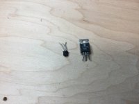
The only input transistors that go bad over time for no reason are this type of TO-92, with the little round flange at the bottom. There are a handful of these types that manufacturers loved to use but they all go bad. It’s an air cavity package like the original TI TO-220 beside it. Fully encapsulated TO-92s didn’t have that problem. Moisture gets in, contaminates it, gets noisy as hell. Are the A539’s like this?
The only input transistors that go bad over time for no reason are this type of TO-92, with the little round flange at the bottom. There are a handful of these types that manufacturers loved to use but they all go bad. It’s an air cavity package like the original TI TO-220 beside it. Fully encapsulated TO-92s didn’t have that problem. Moisture gets in, contaminates it, gets noisy as hell. Are the A539’s like this?
Attachments
It seems we've been here before - about a year ago: https://www.diyaudio.com/community/threads/nec-2sa539-transistor-replacement-equivalent.380299/ Were the replies unsatisfactory at the time?
Last edited:
Hi wg_ski, I’m going replace the pots with some decent ones and try to determine the wiper fail safety resistor values and eliminate that possibility. The LTP devices do not have the flange.
Ian, I only received (or could only see) one reply, a recommendation for the A1015. It had an fT of less than half the specified part, so I felt it was harmless to inquire again. Frankly, with what I’ve learned here I’m glad I did.
Ian, I only received (or could only see) one reply, a recommendation for the A1015. It had an fT of less than half the specified part, so I felt it was harmless to inquire again. Frankly, with what I’ve learned here I’m glad I did.
Last edited:
I would fit the BC556's you have. It's an old and basic design, it is what it is but it has obviously worked OK for all these years and just suffered a natural one off failure.
If the DC offset adjust pre-set is one ended then first just swap the two input transistors around and see if that improves it or not. If not just try another BC in just one of the locations. The input stage isn't a precision DC arrangement as designed.
If the DC offset adjust pre-set is one ended then first just swap the two input transistors around and see if that improves it or not. If not just try another BC in just one of the locations. The input stage isn't a precision DC arrangement as designed.
In circuits like this the fT just isn’t critical. Lower noise is desirable, but any good modern part like the BC5xx will work. Likely lower noise than the original. Just watch the pin outs.
That DC offset adjust is crude and really not a good way to do it. The output DC might balance at a setting which unbalances the gm or the current in the input pair, resulting in increased distortion.
That DC offset adjust is crude and really not a good way to do it. The output DC might balance at a setting which unbalances the gm or the current in the input pair, resulting in increased distortion.
I want to take a moment here to thank each one of you. I greatly appreciate the time and effort put into sharing ideas.
At the suggestion, I've started reading Doug Self's "Distortion in Power Amplifiers". I have his preamplifier from Linear Audio issue #5 awaiting a few parts for completion.
Back to the problem child amplifier, I have some o-ring sealed cermet pots, Nidec CT6EX102 and 501, in 1k and 500R rated 0.5W. I also have some ONSemi BC556BTF transistors.
I think the first step is to remove the old pots and rule out that problem. At the front end of the amp at pot R659, I'm not certain what value or connection method is appropriate for adding a safety resistor, so I've drawn "A" and "B" to help further that discussion. I can also introduce a resistor called "C" to the base of Q1 from between pot R675 and D653, so that if the wiper loses contact the bias doesn't runaway. I'm not certain what values would be acceptable.
Attachments
I'm going to say (lol)... leave it original. Although we do things differently today, the original is fine, its worked all these years and modern parts are magnitudes better. You'll never see the new preset fail. Keep to the original concept.
Be sure to set the bias preset to minimum bias before powering up (wiper connecting to the diode).
Be sure to set the bias preset to minimum bias before powering up (wiper connecting to the diode).
I put a DMM on bias pots to see where they were.
Right channel (problem channel in previous diagrams):
1248 Ohms across bias potentiometer R675, in circuit.
1298 Ohms from base of Q1 to diode D653, and 538 Ohms from base of Q1 to R677. It seems pot R675 has a lot of contact resistance.
Left channel:
1169 Ohms across bias potentiometer R676, in circuit.
1020 Ohms from base of Q2 to diode D654, and 285 Ohms from base of Q2 to R678.
The amp stage was biased by a shop near full deflection on both channels, away from D653. Output devices Q3 and Q5 operated at room temperature, but the Q657 and Q683 ran hot.
I'll start with the new pot's wiper set towards the diode for min bias and adjust for 20mA. R691 + R693 (0.47 + 0.47) = 0.94 Ohms. I*R=V, so 20mA*0.94 Ohms =18.8mV across the two emitters, or 9.4mV across one emitter.
Be sure to have no load attached when setting the bias current. Any slight DC offset can skew the result.
I would also advise using a DBT (bulb tester) when powering up initially.
I would also advise using a DBT (bulb tester) when powering up initially.
Thanks Mooly. The new potentiometers were installed and the amp was brought up with no load or preamp, at minimal bias, and the current consumption was very low. This amp runs with +/- 38.1V DC mains.
Ambient temperature was 19-20 degrees C.
After 10 minutes the heatsink arose 1deg, devices all arose 5deg, with the exception of 2 devices on the problem R channel:
Q651 and Q657 arose 6deg. I couldn't get the laser near Q1 due to it's location between the main output devices.
Deflection of the DC offset pots is the same for each channel, so that seemed promising.
The left-CH DC offset was set after 1min and remained where I set it, varying less than 1mV.
The right-CH DC offset moved up and down 1mV p-p each second and slowly settled to a more negative value (moved -20mV over 10 minutes).
A huge part of the problem was likely as steveu and wg_ski said. The potentiometer for DC offset on the R channel was especially loose. With the pots in hand, I could move the center terminal and get the wiper on either of them to go open circuit. These were exposed wiper pots. I had this problem with the original open wiper pots and the shop replaced them and it went for a decade.
I think there is still a little more going on, though and I'd like to get a 100MHz 2+ CH scope that automatically scales to input signals.
The offset values you measure sound pretty good for such a design. Even an offset of -/+100 mv would not be a problem and historically was the sort of value many amps worked to. If you hold a finger on just one or other of the differential input pair (to warm one or the other) then you will likely see the offset suddenly shift one way or the other... which is all normal.
- Home
- Amplifiers
- Solid State
- 2SA539 Transistor Replacement