hello, i want to ask you about this schematic, what do u guys think.
Im very far from being an a real doityourself-er , i like to play around the pcbs and caps and transistors, but i cant really debug a schematic or to design a circuit.
i have the opportunity to get the pcbs for this and im curious if its worth spending my time and of course my money for this.
please let me know what you guys think.
Attachments
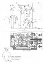
Looks OK. If you're looking for an explanation of how it works (working left to right)
R₁ - protection resistor. Might not save T₁ against worst abuse, but is still useful.
C₁ - DC blocking capacitor. In case input has a DC component.
C₂ - HF shunt, again in case the input has some HF on it, or if there's feedback.
R₂ - Our basic “input impedance” (and ground pulling) resistor.
T₁, T₂ - the first "long tailed pair" or a differential balanced amplifier stage
T₃ - a constant current source.
R₆ - sets the current (relative to D1, D2 and the drop of T₃)
R₅ - raises nominal fixed current to something near GND between +Vcc and -Vcc
R₇ - provides bias for T₃, and current into its base.
D1, D2 act as a poor man's low voltage volt-reference. About 1.4 V for both together.
PR₁ - sets the balance of nominal current between T₁ and T₂
R₃ - current-to-voltage conversion resistor. Current gain of T₁ determines volt gain.
R₄ - same. Opposite side. Constant current results in T₂'s current gain being opposite T₁
R₈ - output negative feedback (NFB) attenuation resistor along with R₉
R₉ - part of R₈-R₉ voltage divider. ¹/₅₀ out back to input. –33 dB attenuation.
C₆ - high frequency damping. HF is always a problem in differential amps.
T₄, T₅ … same as T₁, T₂ - differential or "long tail" pair
R₁₀ - poor man's current-sharing resistor.
The complex of (R₁₄, D3, R₁₁, C₈, T₇, R₁₅, R₁₃, PR₂, R₁₂) produces an indexed (but in phase) version of T₅'s output as well as symmetric loading. The 'how' is beyond this little write up.
T₆ provides clamped voltage difference between its collector and emitter. This is necessary for driving the output transistors.
T₈ (taken by itself) is the “emitter follower” which transforms the relatively high impedance amplification of T₅'s output down to a MUCH lower impedance, suitable for driving output transistors T₁₀ and T₁₁.
T₉ (in compliment to T₈) is doing exactly the same thing, but is flipped upside down. If (conceptually) T₈ is in charge of dragging the output line UP, then T₉ is in charge of dragging it back down. Complimentary pair.
R₁₈, R₁₉ - protecting T₈ and T₉ from excessive base current, and linearizing their emitter-follower behavior.
R₂₈ - providing nominal load to T₈ and T₉, to also have a nominal voltage drop between them.
T₁₀ + T₁₁ … doing exactly the same thing as T₈
T₁₂ + T₁₃ … same as T₉
… and both of these pairs are "just in parallel" to increase current handling capacity.
R₂₅, R₂₆, R₂₇, R₂₈ are called "current sharing" resistors, and help their respective transistors not hog the current.
R₂₉ + C₁₃ suck up HF power output. Protection.
R₁₆, R₁₇ decouple all the high power output power swings from getting into the sensitive parts to the left. Along with C₃ and C₅.
And that's about that.
If you get a PCB and find all the parts, it ought to work.
ITS PROBLEMS - aren't huge, but it has no short-circuit output protection. No over-temperature protection. No soft-on startup. Little quenching of HF feedback (or its OK … there's a few extra caps in the right places to do this.) The R₁₆ + R₁₇ plus downwind capacitors aren't going to do a great job at decoupling the feedback-thru-rails problem. And to be sure, LTP (differential pairs) are pretty sensitive to this.
Yet… it very probably works.
Make sure you get some nice BIG heat sinks for the output transistors AND you mount the things so that the fins are well exposed to circulating air (and are slots-aligned-up/down). I've seen many problems with fins mounted sideways, or "on top" like a mop of bad hair.
And be extra careful when hooking up the speakers: there is NO short circuit protection. None.
GoatGuy
Wow , that's more than I expected for a thought about the schematic.
Many thanks for taking your time .
So , do you think it's going to be an nice amp?
I do know about those non protections(that's why I am still stuck with lm3886/3875/4780 - they do sound good , but I feel like trying some more), thank you for pointing that to me.
Many thanks for taking your time .
So , do you think it's going to be an nice amp?
I do know about those non protections(that's why I am still stuck with lm3886/3875/4780 - they do sound good , but I feel like trying some more), thank you for pointing that to me.
Gabe, do me one small consideration: reread what I wrote enough times in the next few days so that it kind of makes sense. I spent the hour writing it, so that you might really benefit. Call it a "free bonbon".
NICE? It looks OK. It has NFB for both gain control and linearization (lowering inherent distortion). It has a curious indexed difference section, but it looks good. No issues. It uses a totally standard 'emitter-follower driving an emitter-follower' for the output. It uses bog-standard complimentary (PNP, NPN) transistors on the output.
NICE? I can't say beyond that. Nice and linear! Nice and powerful! Yes to both. I'm not sure that for audiophiles tho' that that means 'nice' in some metaphysical sense. Buy a board, take a chance. The fun is often just in the making and 'first watt'.
Lastly - although I do not recommend it up front (after you get your boards) - I do recommend making a couple of modifications. See R₁₆ up there at the top and R₁₇ at the bottom (along with C₃ on top, C₅ on bottom)? They decouple the output from the input.
I would add another set between T₄, T₅ and T₁, T₂, T₃ of the same values, both at the top, and at the bottom. Further decoupling.
The problem of course is that it is NOT your pcb, so you have little-to-no control over the topology. While I would definitely upgrade it (if it was my drawing) to have short-circuit protection, and the additional filtering, without that it is just kind of a "useful crystal" which is hard to change.
So again… buy it, build it. REREAD what I wrote until it makes some sense. ASK questions on the forum for additional explanations. If you ask too many people will point you "to some books" to learn from. Don't feel chagrinned: just get the darn books and learn. And ask. And expect snarky answers from Lone Goats and other denizens of this free-for-all.
In advance: You're welcome.
GoatGuy
Looks OK. If you're looking for an explanation of how it works (working left to right)
R₁ - protection resistor. Might not save T₁ against worst abuse, but is still useful.
C₁ - DC blocking capacitor. In case input has a DC component.
C₂ - HF shunt, again in case the input has some HF on it, or if there's feedback.
R₂ - Our basic “input impedance” (and ground pulling) resistor.
T₁, T₂ - the first "long tailed pair" or a differential balanced amplifier stage
T₃ - a constant current source.
R₆ - sets the current (relative to D1, D2 and the drop of T₃)
R₅ - raises nominal fixed current to something near GND between +Vcc and -Vcc
R₇ - provides bias for T₃, and current into its base.
D1, D2 act as a poor man's low voltage volt-reference. About 1.4 V for both together.
PR₁ - sets the balance of nominal current between T₁ and T₂
R₃ - current-to-voltage conversion resistor. Current gain of T₁ determines volt gain.
R₄ - same. Opposite side. Constant current results in T₂'s current gain being opposite T₁
R₈ - output negative feedback (NFB) attenuation resistor along with R₉
R₉ - part of R₈-R₉ voltage divider. ¹/₅₀ out back to input. –33 dB attenuation.
C₆ - high frequency damping. HF is always a problem in differential amps.
T₄, T₅ … same as T₁, T₂ - differential or "long tail" pair
R₁₀ - poor man's current-sharing resistor.
The complex of (R₁₄, D3, R₁₁, C₈, T₇, R₁₅, R₁₃, PR₂, R₁₂) produces an indexed (but in phase) version of T₅'s output as well as symmetric loading. The 'how' is beyond this little write up.
T₆ provides clamped voltage difference between its collector and emitter. This is necessary for driving the output transistors.
T₈ (taken by itself) is the “emitter follower” which transforms the relatively high impedance amplification of T₅'s output down to a MUCH lower impedance, suitable for driving output transistors T₁₀ and T₁₁.
T₉ (in compliment to T₈) is doing exactly the same thing, but is flipped upside down. If (conceptually) T₈ is in charge of dragging the output line UP, then T₉ is in charge of dragging it back down. Complimentary pair.
R₁₈, R₁₉ - protecting T₈ and T₉ from excessive base current, and linearizing their emitter-follower behavior.
R₂₈ - providing nominal load to T₈ and T₉, to also have a nominal voltage drop between them.
T₁₀ + T₁₁ … doing exactly the same thing as T₈
T₁₂ + T₁₃ … same as T₉
… and both of these pairs are "just in parallel" to increase current handling capacity.
R₂₅, R₂₆, R₂₇, R₂₈ are called "current sharing" resistors, and help their respective transistors not hog the current.
R₂₉ + C₁₃ suck up HF power output. Protection.
R₁₆, R₁₇ decouple all the high power output power swings from getting into the sensitive parts to the left. Along with C₃ and C₅.
And that's about that.
If you get a PCB and find all the parts, it ought to work.
ITS PROBLEMS - aren't huge, but it has no short-circuit output protection. No over-temperature protection. No soft-on startup. Little quenching of HF feedback (or its OK … there's a few extra caps in the right places to do this.) The R₁₆ + R₁₇ plus downwind capacitors aren't going to do a great job at decoupling the feedback-thru-rails problem. And to be sure, LTP (differential pairs) are pretty sensitive to this.
Yet… it very probably works.
Make sure you get some nice BIG heat sinks for the output transistors AND you mount the things so that the fins are well exposed to circulating air (and are slots-aligned-up/down). I've seen many problems with fins mounted sideways, or "on top" like a mop of bad hair.
And be extra careful when hooking up the speakers: there is NO short circuit protection. None.
GoatGuy
+1

Using sluggish MJE340/350 in that "balanced" Voltage amplifier stage (VAS) isn't going to be optimal either. You need something fast and linear there with at least 2W dissipation, depending on actual rail voltages. A CRT TV video driver transistor such as Philips BF469/470 series (if you can still buy genuine NOS) or KSC3503/A1381 would be ideal. Note that frequency compensation caps C6, C7 will need adjustment to account for much less internal capacitance than the MJE350 semis, though I suspect these are nominal values anyway, even though they will have quite an effect on sound quality and high frequency stability.
A lot of cheap designs use the MJE pair but IMHO, it would waste the capabilities of these power output stage semis, not do use more appropriate parts.
A lot of cheap designs use the MJE pair but IMHO, it would waste the capabilities of these power output stage semis, not do use more appropriate parts.
Last edited:
- Status
- This old topic is closed. If you want to reopen this topic, contact a moderator using the "Report Post" button.
- Home
- Amplifiers
- Solid State
- 100-200watts discrete amplifier