Hi,
I just came across the service manual for the a family of Kenwood CD-Changers
kenwood_1060cd_1070cd_d-r350_dp-r6090_7090_sm.pdf
which is available for download at electrotanya.
It seems they have a chip to compute the bitstream and then two 74HC373 per channel, directly followed by the opamps.
What are the advantages of using external logic gates for output switches and downsides? Why would they use D-flipflops? One would assume it is the preceding chip's business to get the timing right, so if they wanted to get the switches off the substrate, a HC04 or HCU04 should have done the job.
Attachments
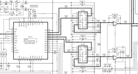
Isn't the 74HC373 a 20 pin Octal Three or Tri-State latch? Those on the diagram are something else by the look of it.
You commonly saw CMOS type switches such as 4053's used after DAC's in the early days of CD.
You commonly saw CMOS type switches such as 4053's used after DAC's in the early days of CD.
Those flip flops look like HC74s, at least the pinout matches my memory.
Right you are, according to the parts list, they are TC74VHC74FE. There was a picture of a 373 to the side of the schematic but not of a 74 so I lazily assumed it was a 373.
Curious, since VHC are known to be a nono in mixed signal engineering because they are extremely noisy (on the supply, but also in terms of EMI radiated from the output leads).
You commonly saw CMOS type switches such as 4053's used after DAC's in the early days of CD.
The switches were used for analog attenuators.
The switches were used for analog attenuators.
I've seen them used for time multiplexed DAC's as well (early players with a shared DAC between L and R channels). The early Sony's come to mind like the CDP101 and the D50 portable.
The DAC would output the voltage sample for one channel and pass it to the appropriate analogue stage, then isolate that stage and calculate the other channels sample value and pass that to that channel in turn.
Attachments
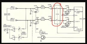
Yes, that was another application. BTT, this is a 1 bit modulator that for some reason uses off substrate VHC logic as its output stage. Why would anyone choose to do that?
I'd guess for the same reason that discrete R2R DACs use 'discrete' logic when the processing's done on an FPGA - power supply and ground noise. I noticed dCS went from multiple gates on a chip to single gate per chip in one of their DAC upgrades years ago - must be the same principle in play.
Only the manufacturer and designers could answer that one. Decisions are made that when looked at years later might seem odd, but there would have been good reason I'm sure when this was done at the time.
Well, it was intrigueing, because I had never seen an audio 1 bit DAC implemented in this way (well, there is the Philips DAC 7 combo, SAA7350 or TDA1307 modulator in CMOS and TDA1547 switcher on a bipolar process, but that is a dedicated switcher rather than a standard logic gate).
There is a suprising amount of playfullness and well-intentioned, but misguided thinking to be found in old commercial designs.
The two CD-players that I have analyzed and modfied speak volumes. The Philips CD 931 PCB must have been designed by an intern who had not read the mixed signal tutorials from Analog Devices and other IC manufacturers. Two sided PCB with top side as dedicated ground plane, but no effort to separate digital and analog grounds and to minimize loop areas. The TEAC CDP 3000 had a handfull of ceramic caps scattered around the board for supply decoupling with absolutely no thought given as to what ground the decouple into. A beancounter would have replaced them with one cap for every ten, and a good engineer would have placed them where the benefit was to be had.
Such 1bit DAC need clean power supply because it is the DAC reference, i.e. the noise on the PSU almost goes through to the DAC output. 1bit DACs such as cirrus, sony, JVC had separate supply pins for the reason (and even recent ES90xx and AK4499). Else you can separate the back-end of the DAC.
Separating back-end also let the IC substraight (gnd) and clock pin if wanted, separate thus less susceptible to digital noise. Downside is it is not able to control Pch and Nch matching of the output gate (monolithics can). Recent in-house discrete dacs are generally consist of FPGAs and D-FFs, such as chord, marantz SA-10, esoteric D1X K1X.
Sony's later 1bit DACs (current pulse DACs) had flip flop with current mode output.
Hi,
I just came across the service manual for the a family of Kenwood CD-Changers
kenwood_1060cd_1070cd_d-r350_dp-r6090_7090_sm.pdf
which is available for download at electrotanya.
It seems they have a chip to compute the bitstream and then two 74HC373 per channel, directly followed by the opamps.
What are the advantages of using external logic gates for output switches and downsides? Why would they use D-flipflops? One would assume it is the preceding chip's business to get the timing right, so if they wanted to get the switches off the substrate, a HC04 or HCU04 should have done the job.
They are nothing else than reclockers.
Presumably those separate flip-flops are there to reduce supply, ground and substrate coupling from all the digital logic in IC11 to the analogue signal, although I don't see a separate clean supply for the 74VHC74 on the schematic. The flip-flops are indeed the DAC, not IC11. As it is a non-return-to-zero DAC, the flip-flops need to have very little difference between the tPLH and the tPHL.
I notice they parallel the flip flop outputs for more current too(!) - presumably the choice of
chip at the time was based on speed/jitter and drive capability considerations.
chip at the time was based on speed/jitter and drive capability considerations.
- Home
- Source & Line
- Digital Source
- 1 bit dac made from 74HC373 D-Flipflops?