Hi,
I build some amps with voltage followers output. They all produce some amount of crossover distortion (because of imperfect BE output pair compensation) that is hearable at low volumes.
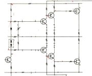
Few days ago I come up with common emitter output that is designed to work at high quiescent current (consider 200mA for now).
When positive wave on input appears the Q5 supplies a 300mA (as example) , the Q6 sinks just 100mA and 200mA flows to Load.
This should ensure the both transistors are always biased and no crossover should appeared.
Of course the high quiescent current is not a power efficient but for small room low power amp it’s ok.
Do you have some other ideas how to avoid crossover?

Recorded sound by phone-camera:
https://www.facebook.com/reel/2757148411128631/?mibextid=rS40aB7S9Ucbxw6v
I build some amps with voltage followers output. They all produce some amount of crossover distortion (because of imperfect BE output pair compensation) that is hearable at low volumes.
Few days ago I come up with common emitter output that is designed to work at high quiescent current (consider 200mA for now).
When positive wave on input appears the Q5 supplies a 300mA (as example) , the Q6 sinks just 100mA and 200mA flows to Load.
This should ensure the both transistors are always biased and no crossover should appeared.
Of course the high quiescent current is not a power efficient but for small room low power amp it’s ok.
Do you have some other ideas how to avoid crossover?
Recorded sound by phone-camera:
https://www.facebook.com/reel/2757148411128631/?mibextid=rS40aB7S9Ucbxw6v
Last edited:

Welcome to diyAudio!
You basically made a class A amplifier. Ian Hegglun once came up with a somewhat more efficient variant he calls square law class A. He takes the difference between the currents through two devices with a more or less quadratic response.
When you just want to keep the output transistors from switching off, you can also do what is usually called non-switching class AB. For example, "Audio power with a new loop", Electronics World February 1996, pages 140...143, https://worldradiohistory.com/UK/Wireless-World/90s/Electronics-World-1996-02-S-OCR.pdf
Thank you MarcelvdG , I will check this article.
I forgot to add an output measurement, so I place it here:

I forgot to add an output measurement, so I place it here:
This question has received a century of work.Miso156 said:Do you have some other ideas how to avoid crossover?
Only class A can avoid crossover distortion (a practical amplifier will have other non-linearities).
Class AB relies on non-linearity for its operation. The non-linearity can be minimized. You may be interested in my article on Class AB Biasing.
Ed
Notice this circuit delivers less than 2W RMS into 8 Ohms. Not much from a 2n3055/2955 pair. It's not difficult to make a class-AB that gets better than 0.01% THD, perhaps 0.001% and if you can hear that then you have better ears than I.
 Welcome to diyAudio!
A striking resemblance with another variation of this output stage, with the V-fet output by Sony (4650), in clearified view.
At the same time, the output config is just different, but the scope is similar: one needs a high current capable collector or drain output stage to avoid this nasty switching. Done with modest components (2955/3055), 2W@8 is an achievement nonetheless.
Being Q3-Q5 & Q4-Q6 in a Sziklai mode, thermal coupling is on debate now!
Attachments
In the schematic of post 1 no useful amp is described, because most
of the output power is wasted in R11 and R12. I suspect unpleasant
operation at high amplitude levels also.
The output as shown, without any feedback, has high output impedance,
it has current source character.
The comparison with the Sony amp, post 7, is not justified, have a look
at the wiring re ground and output.
I recommend you buy and read the Douglas Self book. https://www.amazon.com/Audio-Power-Amplifier-Design-Sixth/dp/0240526139 Self does an excellent job of describing, building testing and documenting the performance of many variations of each amplifier stage. In the book he shows the design of a very high performance class B amplifier. This isn't audiophile magazine bs, it's all real world engineering with example circuits and test results that can be reproduced by those skilled in the art.
I suppose you might look at a class D amplifier. Those do not appear to suffer from crossover distortion as they operate the same across the voltage output swing of the amplifier.
It is also very informative to characterize your hearing. It very often isn't nearly as exotically super accurate as many people believe it to be. This website will bring you back to reality. https://www.audiocheck.net/
Yes, the designations are wrong, the schematic not.FWIW you swapped the 2N3055 and 2N2955 in the final stage
All true, but not the aim of the op. Nor the actual valid config.In the schematic of post 1 no useful amp is described, because most
of the output power is wasted in R11 and R12. I suspect unpleasant
operation at high amplitude levels also.
The output as shown, without any feedback, has high output impedance,
it has current source character.
The comparison with the Sony amp, post 7, is not justified, have a look
at the wiring re ground and output.
Keen eye!FWIW you swapped the 2N3055 and 2N2955 in the final stage
Turning back to known islands into an spacious ocean... granted.I recommend you buy and read...
But no further progression though.
The op's proposition & aim is to find an output stage without the dreadfull switching class ab switching distortion. That's the issue, not the known save heavens. Challenge.
Thanks for sharing. CFP allows low bias current because it reduces switching noise on site. The P3A is a good example. However phase lag has to be addressed. There's also CFP with an emitter follower. The other topology is quasi complementary, again phase lag issues have to be addressed. Other approaches are non switching topologies for emitter followers, bias 1st watt into class A for emitter followers, high bias class A , Krell et al. There's also Bryston with their compound output stage to address crossover distortion , it does double duty of both current and some voltage gain, its a four stage amplifier in a three stage package. Switching noise reduction is important for low thd amplifiers because it can make them sound unpleasant or non engaging.
An amplifier you need to listen to is the SYMEF.
An amplifier you need to listen to is the SYMEF.
Thx everyone for comments.
I tried to use a lower shunts (6ohm), the amplitude across speaker can go higher. The efficiency is maximal at high volume, at low volumes the energy is waisted on transistors means what Pnp supplies the Npn sinks.
At high volume one of transistor is almost closed so most energy goes to speaker.
The amp is open loop (not perfect approach) but anyway the bias point and gain are well maintained. The amplitude is probably little lost at higher signal levels.
Regarding AB I think the switching can be eliminated but not avoided by increasing a quiescent current or using some more sophisticated approach.
But as I mention, for 2W amp that I need I don’t care about power efficiency, even it will be 40%.
- Home
- Amplifiers
- Solid State
- Avoid a crossover distortion completely