I've been working on rebuilding my Hafler DH-220 into the DH-220C input circuit - the Bob Cordell designed circuit that's sold by delta9electronics on eBay and I believe is a member here.
Anyway...on power-up, (the rail-to-rail voltage is about 120V or just under +/-60V) and it more or less immediately fried R53, the 22 ohm resistor at the positive rail, along with both R13 and R25 the 180 ohm resistor that power Q1 and Q2.
This was only one the right channel - the left channel seems to have survived.
Questions:
I haven't pulled the transistors, but is it safe to assume they're also toast, or is there a chance they're ok.
What would have caused R13 and R25 to burn.
I presume that R53 blew because of overcurrent at R13 and R25...
Where should I be looking for the root cause?
Last edited:
Update - Q13 dead as well as D1.
I'm wondering if D1 is the culprit here as it regulates the voltage for the parts I killed...
I'm wondering if D1 is the culprit here as it regulates the voltage for the parts I killed...
For those who wish to follow along, from Bob's website: http://www.cordellaudio.com/poweramp/DH-220C_MOSFET_Power_Amplifier.pdf
Rick Savas (@rsavas) operates delta9electronics and is a frequent contributor here.
Rick Savas (@rsavas) operates delta9electronics and is a frequent contributor here.
Did you test the boards before connecting the output stage? Bypass the bias network( there’s jumpers on the board to do this).
@ticknpop, yes I did. The output boards were not connected at all and the jumpers were properly set for testing.
Only one of the boards fried, so it must have been an assembly or part selection issue, or one of the parts was bad to begin with.
At this point, I'm looking for advice on what to check before powering up again.
Only one of the boards fried, so it must have been an assembly or part selection issue, or one of the parts was bad to begin with.
At this point, I'm looking for advice on what to check before powering up again.
So far I have found the following failed components:
R53 (not shown on schematic but in line with +V(rail)
R13
R25
Q6
Q13
D1 (also not shown but is the shunt zener +15V regulator)
It's weird. I can't see R53 burning unless there was a large amount of current (which of course there was). R13 and R25 saw enough current to blow, and Q6 is in line with R25, but Q13 is inline with R25, which was perfectly fine, so I guess Q6 was fully conducting which put over voltage on the base of Q13? Am I reading the schematic right?
D1 is also fishy...it was blown, but I wonder if it is the root cause of all the issues...
If it is bad from he start then the +15V reference at the bases of Q6 (blown) and Q14 (OK) would have been potentially too high.
I'm rambling here trying to talk myself into finding the root cause, but I can't figure out what it would have been...
First check all Resistors and diodes by unsoldering one leg or without. Then go from Q2 and Q7. I would de-solder two legs of the transistor for checking using diode functions. Then remove the suspects and check out of the circuit Did you check the terminals of the transistors before soldering them? I always keep epay transistor checker to verify terminals before soldering them as well correct type.
I've traced down the positive side of the circuit checking all the resistors (multimeter) and transistors all the way down to and including the FETs, which all tested "good" (and all the PNP bipolar transistors all returned similar values) on one of those universal parts checkers you find on online reseller sites. Apart from the found bad components, that is...
I think all that is left to to is wait for replacements and try again with fingers crossed....
I think all that is left to to is wait for replacements and try again with fingers crossed....
An initial power up test of the AFE using a current limited supply might have saved part destruction and identified a malfunction.
Not having a current limited +/-supply could be substituted with a couple of 100ohm power resistors in series with supply inputs
Not having a current limited +/-supply could be substituted with a couple of 100ohm power resistors in series with supply inputs
The one thing that's conspicuous by its absence is a decent bipolar bench power supply. Or a pair of supplies I can connect in series to get +/- voltages. If you have a suggestion for a particular model(s) I'm all ears.
To add to my nostalga HP test equipment setup I recently bought an old HP6227B +/- 50V ADJ V/I PS from our popular auction site. A HP6228B sits right beside it. l like the analog meters, don't care that the V meter is not very accurate, have a HP 3478A for that. Checking the service/schematics on these, I found out that they use an old RCA CA3026 is a TO can package version of the DIP CA3053? More nostalgia.
Update on this project.
I believe that I found the root cause of the failure of the IPS board.
Zener diode D1, which provides the +15V reference, was either bad from the start or failed on startup and caused the failure of the above listed components, including Q8, which was partially shorted - it tested ok in a tester, but a multimeter test across C to E showed only 147 ohms, so it was bad.
Ok...all other components tested fine, replacements were installed and it was powered up successfully, and biased properly and predictably according to the instructions.
Time to connect the OPS board.
No problems there either. It also powered up without incident and I was able to set the IPS bias predictably on both channels to the required 40 mV across the test points corresponding to 400 mA. Nice.
I then connected a pair of test speakers, and slight buzz from the right channel. But there was nothing connected at the input.
So I powered down and as it discharged its reservoir capacitors I heard a oscillatory buzz as the reservoir caps finally bottomed out. This is a bit concerning, but I connected a source to the inputs anyway.
I actually got sound out of the amplifier, but only very briefly - like less than two seconds and it immediately smoked a resistor on the OPS board and another on the IPS/VAS board. And they were not ones that you'd expect.
On the IPS board, resistor R3 blew on both channels.
R3?? come on, that's the resistor that ties signal ground to the chassis. And something caused it to blow, so that meant significant current was attempting to drain into the chassis.
But what could that be??
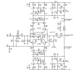
In a similar vein, on the OPS board (diagram shown) resistor R2 blew on both channels. And fairly spectacularly. Again, that ties the output ground to the chassis, so something was passing significant current there, too. But what??
I can't think of what it could be. Could the chassis have become energized with something? It's not from the MosFETs. I did check to see if they were isolated (they were).

Has anyone experienced anything like this?
Also, what is the purpose of these low value resistors from signal ground to the chassis?
I believe that I found the root cause of the failure of the IPS board.
Zener diode D1, which provides the +15V reference, was either bad from the start or failed on startup and caused the failure of the above listed components, including Q8, which was partially shorted - it tested ok in a tester, but a multimeter test across C to E showed only 147 ohms, so it was bad.
Ok...all other components tested fine, replacements were installed and it was powered up successfully, and biased properly and predictably according to the instructions.
Time to connect the OPS board.
No problems there either. It also powered up without incident and I was able to set the IPS bias predictably on both channels to the required 40 mV across the test points corresponding to 400 mA. Nice.
I then connected a pair of test speakers, and slight buzz from the right channel. But there was nothing connected at the input.
So I powered down and as it discharged its reservoir capacitors I heard a oscillatory buzz as the reservoir caps finally bottomed out. This is a bit concerning, but I connected a source to the inputs anyway.
I actually got sound out of the amplifier, but only very briefly - like less than two seconds and it immediately smoked a resistor on the OPS board and another on the IPS/VAS board. And they were not ones that you'd expect.
On the IPS board, resistor R3 blew on both channels.
R3?? come on, that's the resistor that ties signal ground to the chassis. And something caused it to blow, so that meant significant current was attempting to drain into the chassis.
But what could that be??
In a similar vein, on the OPS board (diagram shown) resistor R2 blew on both channels. And fairly spectacularly. Again, that ties the output ground to the chassis, so something was passing significant current there, too. But what??
I can't think of what it could be. Could the chassis have become energized with something? It's not from the MosFETs. I did check to see if they were isolated (they were).
Has anyone experienced anything like this?
Also, what is the purpose of these low value resistors from signal ground to the chassis?
Attachments
Might be worth the while to build (or otherwise acquire) a dim bulb tester if you're not using current-limited supplies for testing.
Did you check to insure that your MOSFETs are galvanically isolated from the heat sinks? I beleive for TO-3 package lateral MOSFETs, the drain is tied to its case.
And you checked the PCB for solder bridges, stray pieces of wire leads from trimmed components, etc.?
You've checked that you're using correct semiconductor polarities in the right places?
I believe everything is correct. I checked all the mosfets and they are not shorted to the chassis. When I rebuilt the chassis it got new mica insulators and new mosfet sockets.
And I did start it up with a dim bulb tester and it started smoothly and passed the biasing tests described in the AudioXpress article without incident. The IPS reproduced a 10KHz square wave very nicely well past 3VRMS at the test point.
The issue happened when speakers were connected and an input signal applied.
- Home
- Amplifiers
- Solid State
- DH-220C project - power up...smoke!