Should I just give up?
I've been trying to figure out why the dc offset is so high on this old amp, it's on both channels.
Things I've done:
Closely matched the LTP c1815's and the a949's. I have a few NOS of these so they are not the fakes.
All resistors are 1% and very close match, of course except R8,15,16,17.
All electro caps are new and are Panasonics or Elna.
The Finals are good.
The bias I have it at 20 or 25 mA
It plays music OK.
Only thing I can think of trying is replacing R7 (1.5k) with a 2k multi turn pot and try to adjust it for 0dc offset.
The last few days I've been reading just about everything on LTP, current mirrors, VAS...Ugh.
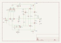
I figured I draw the schematic and maybe someone can see something I'm missing and before I try the multi turn pot idea.
Please be as harsh or as nice as you want... I can take it...
Scott
I've been trying to figure out why the dc offset is so high on this old amp, it's on both channels.
Things I've done:
Closely matched the LTP c1815's and the a949's. I have a few NOS of these so they are not the fakes.
All resistors are 1% and very close match, of course except R8,15,16,17.
All electro caps are new and are Panasonics or Elna.
The Finals are good.
The bias I have it at 20 or 25 mA
It plays music OK.
Only thing I can think of trying is replacing R7 (1.5k) with a 2k multi turn pot and try to adjust it for 0dc offset.
The last few days I've been reading just about everything on LTP, current mirrors, VAS...Ugh.
I figured I draw the schematic and maybe someone can see something I'm missing and before I try the multi turn pot idea.
Please be as harsh or as nice as you want... I can take it...
Scott
Attachments
If the DC output voltage is negative and the input transistors are from one of the lower hFE groups, it could simply be the base currents causing more DC voltage drop across R1 than across R4. Like Nigel, I also don't think it will do any harm.

Try a 12k resistance for R1, as pointed by MarcelvdG R1 unbalance with R4 is possibly the culprit, if output offset doesnt decrease then it means that the currents are not well distributed in the LTP from the start.
That being said 150mV in a speaker whose DC impedance is say 4R will result in a 37.5mA current and 5.6mW dissipated by the speaker, nothing to worry about on a reliabilty point of view.
That being said 150mV in a speaker whose DC impedance is say 4R will result in a 37.5mA current and 5.6mW dissipated by the speaker, nothing to worry about on a reliabilty point of view.
Thanks much.... Now more to try...
So I think R4 and R5 set up the gain and I think it's about 20dB. And I see what your talking about with R1 (47k) and R4 (12k). With this in mind, would changing R4 to 47k and R5 to 2.3k, would still be about 20dB of gain or am I thinking wrong?
So I think R4 and R5 set up the gain and I think it's about 20dB. And I see what your talking about with R1 (47k) and R4 (12k). With this in mind, would changing R4 to 47k and R5 to 2.3k, would still be about 20dB of gain or am I thinking wrong?
I agree that 150mV offset is safe to ignore, but you can easily trim out the error if you wish.
I’m assuming the offset is negative as Marcel explained in post 3. So you need to inject a small current to raise the offset error 150mV: = 0.15V/12k = 12.5uA. So install a resistor between the negative rail at C3 and C6; the voltage across this resistor will be about 32V. Its value should be 32V/12.5uA = 2.666M. So try a 2.7M resistor.
BTW, I believe C6 may be installed with the wrong polarity.
Thanks much.... Now more to try...
So I think R4 and R5 set up the gain and I think it's about 20dB. And I see what your talking about with R1 (47k) and R4 (12k). With this in mind, would changing R4 to 47k and R5 to 2.3k, would still be about 20dB of gain or am I thinking wrong?
It s easier to trim R1 because R4 has C5 in parralel and that would change the impedance ratio between R4 and C5.
Changing R4/R5 would require to resize C5 accordingly, not counting that a higher value for R5 would increase slightly the amp noise.
You could trim R2 up or down a bit.
That would be the second step if even R1 = R4 does not work, otherwise triming R2 would result in an unbalanced current
in the LTP if the offset is actually due to R1/R4.
The amp has gain of 1 at DC due to C6. That's why wahab suggested 12k for R1 in post 5. The downside to this is that the smaller value moves the high pass corner frequency (C1 and R1).Thanks much.... Now more to try...
So I think R4 and R5 set up the gain and I think it's about 20dB. And I see what your talking about with R1 (47k) and R4 (12k). With this in mind, would changing R4 to 47k and R5 to 2.3k, would still be about 20dB of gain or am I thinking wrong?
BSST, Thanks. Yes it is a Neg offset. C6 is drawn this way on the PCB and the stock cap when new was this way. Can I put in a NP 100u/6.3v?
DC OFFSET 10mv or less
R4 & R1 need to equal both 12K.
Q1 & Q2 need to be matched and thermally coupled.
Other strange omissions are no base stoppers in Q7 & Q8, no flyback diodes across Q9 & Q10, values of R6 & R7 might be slightly too low?
R4 & R1 need to equal both 12K.
Q1 & Q2 need to be matched and thermally coupled.
Other strange omissions are no base stoppers in Q7 & Q8, no flyback diodes across Q9 & Q10, values of R6 & R7 might be slightly too low?
OK I will try the R1 to 12k and post the results.
Audio1Man, could base stoppers in Q7 & Q8,(not sure what they are), flyback diodes across Q9 & Q10, (1n4___'s across what pins) and values of R6 & R7 increased to 1.7K? I don't mind modding circuits.
Audio1Man, could base stoppers in Q7 & Q8,(not sure what they are), flyback diodes across Q9 & Q10, (1n4___'s across what pins) and values of R6 & R7 increased to 1.7K? I don't mind modding circuits.
Are you sure R6 & R7 are connected that way? Very odd to see the 1st stage LTP 'woven' into the 2nd LTP. It brings down to loop gain, and not doing well in supressing the offset.
Q1 & Q2 should have a small negative voltage at their base.
An offset of 150mV / 12k = 12.5μA 'offset current' running backwards to the 1st LTP.
R2 yields 32V / 22k = 1.5mA, so 0.75mA per leg. That would make bata of Q2 (750μA / 12.5μA =) 60, which is very low.
The base current must be much lower (eg 750μ / 250 = 3μA), so where is that extra current going to?
On Q1, this 3μA * 47k makes -141mV (yes it is negative!), on Q2 this should be 3μA * 12k = +36mV higher; the offset should be -105mV (in perfect balanced conditions though).
C1 & C6 are not happy with that (small) negative voltage. And should be bipolars.
edit: lots of posts while typing...
Yes, I'm sure R6,7 are this way. So I've looked at other amp schematics and most if not all have the R1 and R6 equal in value.
I will try this, R1 to 12k and should I change the value of C2? Up or Down? I have the supplies.
I will try this, R1 to 12k and should I change the value of C2? Up or Down? I have the supplies.
THANKS MUCH YOU GUYS. You all are so very helpful and you don't have to be. That is so very kind.
I should have pursue'd an engineering degree. All I have is an associates in electronics.
I should have pursue'd an engineering degree. All I have is an associates in electronics.
Doubtfull, never seen that the last 40 odd years. Post a picture of the pcb, top & btm sides.Yes, I'm sure R6,7 are this way.
Ehmm... typo and/or assumption?I've looked at other amp schematics and most if not all have the R1 and R6 equal in value
edit: R6&R7 are not connected as in #1, it's impossbile. It's hardshortening the loop gain.
It's to be expected: ~30V/R2= 1.36mA /2 = 682uA /Beta about 100 = 6.82uA *(R1-R4=35K) = 238mV offset, so the LTP Beta must be closer to 200. The LTP VAS is unusual and perhaps a bit misguided, but it should not be your problem. I would probably modify it into a "Blameless" topology but then it's no longer to same amp. I would add some basic current limit protection.
- Home
- Amplifiers
- Solid State
- 1988 Amp with 0.150 vDC offset (150mV)