I have built this 405 clone, but when checking I found it has a large amount of dc volts (26v)at the out+ and case. obviously not right can anyone please point me in the direction of the fault?

sorry I should have said , measured between out+ and the neg speaker terminal.isnt the case supposed to be tied to 0v - thru the h\s
I suggest you post a schematic of your module. It will make it easier for members to offer suggestions.
I wish I could but I dont have one or know where to get oneI suggest you post a schematic of your module. It will make it easier for members to offer suggestions.
You are correct, I dont quite get it, measure from where to where?you dont seem to understand the inference,
is the input 0v at 0v
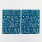
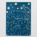
the best I have is some pics of the unpopulated boardI suggest you post a schematic of your module. It will make it easier for members to offer suggestions.
Attachments
You really should try to find a schematic. Debugging without it is a nightmare and fraud with errors.
It will cost some effort but will be worth it.
Jan
It will cost some effort but will be worth it.
Jan
If it uses the LM301 opamp it is likely a derivative of this. Check the opamp supplies are correct on pins 4 and 7.
Check that pin 3 is connected to ground (zero volts). Assuming it is measure the voltage from pin 3 to the speaker output. What voltage do you measure? What voltage do you measure between pin 3 and pin 6. Keep the black meter lead on pin 3 and be sure to record the polarity of any voltages measured.

Check that pin 3 is connected to ground (zero volts). Assuming it is measure the voltage from pin 3 to the speaker output. What voltage do you measure? What voltage do you measure between pin 3 and pin 6. Keep the black meter lead on pin 3 and be sure to record the polarity of any voltages measured.
Pin 3 to spk out =33.9v dc +, pin 7=14.76+, pin 4=13.93, pin 3+6 =12.20+,If it uses the LM301 opamp it is likely a derivative of this. Check the opamp supplies are correct on pins 4 and 7.
Check that pin 3 is connected to ground (zero volts). Assuming it is measure the voltage from pin 3 to the speaker output. What voltage do you measure? What voltage do you measure between pin 3 and pin 6. Keep the black meter lead on pin 3 and be sure to record the polarity of any voltages measured.
View attachment 1118367
Last edited:
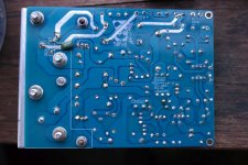
How are the output transistor fixing 'bolts' isolated from the heatsink? Need to see the underside.
the inference was that the input needs to be connected to 0v - (the 2 main capacitors common), i remember sellers on ebay stating this in the listings for the quad kits
measure from the 0v on the main caps to the input -ve !, if this hasnt been wired in then there will be dc on the o\p
that is why there is a crimp connector on the h\s
measure from the 0v on the main caps to the input -ve !, if this hasnt been wired in then there will be dc on the o\p
that is why there is a crimp connector on the h\s
Last edited:
The bolts are isolated from the heatsink with heatshrink tubingHow are the output transistor fixing 'bolts' isolated from the heatsink? Need to see the underside.
Attachments
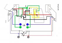
Ok thanks, there are two ground points on this board , one is PGND the other GND. the crimp fitting I put myself in case I had to connect another wire, the amp is earthed as per this diagram from Dada.the inference was that the input needs to be connected to 0v - (the 2 main capacitors common), i remember sellers on ebay stating this in the listings for the quad kits
measure from the 0v on the main caps to the input -ve !, if this hasnt been wired in then there will be dc on the o\p
that is why there is a crimp connector on the h\s
Attachments
I'm completely unfamiliar with Quad 405 amplifiers, but are there errors in this schematic?If it uses the LM301 opamp it is likely a derivative of this. Check the opamp supplies are correct on pins 4 and 7.
Check that pin 3 is connected to ground (zero volts). Assuming it is measure the voltage from pin 3 to the speaker output. What voltage do you measure? What voltage do you measure between pin 3 and pin 6. Keep the black meter lead on pin 3 and be sure to record the polarity of any voltages measured.
View attachment 1118367
Seems like D5 and D6 should lie between bases of TR9 and TR10. There doesn't appear to be a bypass on +50 rail comparable to C18. No supply bypass caps on IC1. D1,R9,R11 hookup seems totally bizarre. Note re R11 is a head-scratcher to my head.

Pin 3 to spk out =33.9v dc +, pin 7=14.76+, pin 4=13.93, pin 3+6 =12.20+,
Pin 4 should be the negative rail for the opamp. Is that (minus) -13.93 you measure? Detail is everything 🙂
Assuming it is negative then you need to look where the 'loop' is failing. A quick and dirty test is to just apply a short across what is C6 in the diagram I posted. That should swing the output to the negative rail.
If you are getting nowhere then I suggest using the diagram I posted as a template for what the circuit should be and for you to measure and write all the key voltages on the transistors and we can see where things are falling apart (hopefully).
I'm completely unfamiliar with Quad 405 amplifiers, but are there errors in this schematic?
It is correct... its a very clever circuit that isn't easy to just figure out at first glance. There were many updates to it and the one I posted is one of the first original variations.
It does all work as expected with zero bias current in the dumpers.
Yes pin 4= 13.93 minusPin 4 should be the negative rail for the opamp. Is that (minus) -13.93 you measure? Detail is everything 🙂
Assuming it is negative then you need to look where the 'loop' is failing. A quick and dirty test is to just apply a short across what is C6 in the diagram I posted. That should swing the output to the negative rail.
If you are getting nowhere then I suggest using the diagram I posted as a template for what the circuit should be and for you to measure and write all the key voltages on the transistors and we can see where things are falling apart (hopefully).
- Home
- Amplifiers
- Solid State
- QUAD 405 clone high DC on output