Hello, I'm new here and this is the first amp I will try to fix. I have SMD soldering and development experience but this is my first time working on an amplifier. Here we have an MMats 6150D, it was working fine before but it let the magic smoke at random once. I opened it up and noticed this:
Clearly, a MOSFET died

I took out the clamps and noticed that 80% of the MOSFETS cracked or burnt on this rank of fets alone, all the other MOSFETS around the amp seem fine.

I cleaned out the smoke residue and noticed two resistors blew, I checked the diodes and they test out fine still. I also noticed the temperature sensor (?) on the upper left has its leads burnt, but I think that is due to the MOSFET nearby producing heat.

So now to gather parts, as I understand when a MOSFET gives out, it takes its driver IC with it but I don't know which one is it


Questions:
Thanks!
Clearly, a MOSFET died
I took out the clamps and noticed that 80% of the MOSFETS cracked or burnt on this rank of fets alone, all the other MOSFETS around the amp seem fine.
I cleaned out the smoke residue and noticed two resistors blew, I checked the diodes and they test out fine still. I also noticed the temperature sensor (?) on the upper left has its leads burnt, but I think that is due to the MOSFET nearby producing heat.
So now to gather parts, as I understand when a MOSFET gives out, it takes its driver IC with it but I don't know which one is it
Questions:
- What's the best MOSFET to use? burnt ones are really faded out but I managed to make out "top line: IRF3205, middle line: I&R P12J, bottom line: 40 CZ"
- What resistors should I use? -markings have been burned out, the only clue I have is a nearby one that is the same physical size with margins "10RD" (or 10R0), everyother resistor is a smaller in physical size.
- What driver IC can I use?
- Anything else I'm missing before I go out and buy parts?
Thanks!
IRF3205 is the relevant part number.
https://octopart.com/search?q=IRF3205¤cy=USD&specs=0
I don't have a definitive value for the resistors that are parallel with the diodes. In a similar amp, they used 24.9 ohm (25 ohm) resistors. When you order parts, also order some 10 ohms. The size is likely 1206.
I can't find the original part number from the markings on the driver transistors(?).
The SG3525 likely survived. The parts that appear to be driver transistors may have survived. For testing (and maybe as a viable solution) the 3525 can drive the PS FETs.
Have you tested the output transistors to see if any failed?
I'd pull the PS FETs and test the drive signal at the FET gates.
Do you have a scope?
-Thank you for the rough resistor value and size. I'll get both 24.9 & 10 ohmIRF3205 is the relevant part number.
https://octopart.com/search?q=IRF3205¤cy=USD&specs=0
I don't have a definitive value for the resistors that are parallel with the diodes. In a similar amp, they used 24.9 ohm (25 ohm) resistors. When you order parts, also order some 10 ohms. The size is likely 1206.
I can't find the original part number from the markings on the driver transistors(?).
The SG3525 likely survived. The parts that appear to be driver transistors may have survived. For testing (and maybe as a viable solution) the 3525 can drive the PS FETs.
Have you tested the output transistors to see if any failed?
I'd pull the PS FETs and test the drive signal at the FET gates.
Do you have a scope?
-Sorry, my memory is a bit rough (don't know what a transistor is on this board), which transistors are you referring to? I can try to get a better image, I just removed the entire board (the bottom look good and there's nothing on it, just some basic traces)
-have not tested the transistors yet
-"I'd pull the PS FETs and test the drive signal at the FET gates." I believe you mean to pull the power supply MOSFETs (broken ones) and test the FET gates, as in the gates on the transistors themselves aka removing the broken MOSFETs and testing their gates? (its been a while since i dealt with these little guys).
-I have an old Fluke that still works, i believe this should work even though is isolated.
I took better pictures in some of the chips in case it helps:
I noticed there's x3 of these by x3 of the vertical cards:


Noticed this one too:


Scope I plan to use, Fluke 199C - 200Mhz, been a while since i used one:

Last edited:
Possible driver (below).
If you're referring to "driver transistors(?)", I didn't know what it was (and still don't definitively). It may be the driver IC below.
Yes, pull the PS FETs before checking the drive signal. You can check the drive up to the output of the components marked 3005 without replacing the burned resistor. It's better to check the drive signal with a load. Any cap between a 0.01uF and a 0.1uF will work well for the power supply.
The isolated scope will work.
Attachments
Last edited:
Great thank you, I was having such a hard time finding that IC because i was including the date code as well. So i ordered the parts from digikey below. for the MOSFET I went with the 110 amp variation instead of 75 amp, which i believe should give me some headroom.

Unfortunately, the lowest capacitors I have at hand are .47Uf so I ordered some.1's Now regarding how to test this IC:

Unfortunately, the lowest capacitors I have at hand are .47Uf so I ordered some.1's Now regarding how to test this IC:
- where do I connect my oscilloscope lead to? Vee, Source, Sink? (other one of course, to GND)
- How do I connect the capacitor to the IC? Im going to use a polarized cap so I drew it on the example circuit chart found on that 3005 datasheet.
- Just making sure, I should have the amp powered on to test this right? so overall:
- remove all 8 burned MOFSETs
- add a capacitor as load
- connect my oscilloscope leads
- power up the amplifier using a 12v regulated power supply
- compare findings from the datasheet and report back here.
I should have been more specific. The loading capacitor should be a ceramic or film capacitor (see attached).
The loading capacitor connects across the gate and source pads of the PS FET. The scope will connect across the cap. Since the 3rd leg (source) is ground, you can connect the scope's ground lead to the primary ground terminal.
The waveform, without the load, will typically be a perfect square wave. With the loading capacitor, it will look similar to the attached waveform. It should swing from ground to approximately 12v.
Did you check the connections for the 3005 to confirm that that's the correct part?
There is essentially no difference between the FETs marked as 75 amp and 110 amp. One is the package limit and the other is the silicon limit. Look up the datasheets. Find the specs at 25C and 100C.
Attachments
Been a little busy so i staged everything for testing but haven't tested yet.
So Im pretty sure I had the needed ceramic caps all along I have some 104 and 103's that i believe are the exact values you mentioned, so i will go with the 104.

Removed all that carnage, the labels are so faded that even then its hard to make out the labels.

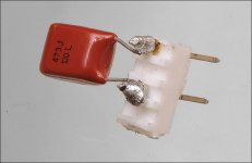
I hope this thermal probe works because i dont know its parts number

Noticed the underside of the board was all covered in old flux i think, i think this is normal.

Cleaned out my flux


Lifted one pad, but i think im ok because the connections are on the top

Removed the blown resistors

Regarding the load testing, this is a mock up, is this were put the capacitor? between the Source and Gate. Or is it directly on the IC?

-Did you check the connections for the 3005 to confirm that that's the correct part?
they seem to match while looking at the little direction marking dot on the IC
-There is essentially no difference between the FETs marked as 75 amp and 110 amp. One is the package limit and the other is the silicon limit. Look up the datasheets. Find the specs at 25C and 100C.
I believe they check out, here snip from its datasheet

So Im pretty sure I had the needed ceramic caps all along I have some 104 and 103's that i believe are the exact values you mentioned, so i will go with the 104.
Removed all that carnage, the labels are so faded that even then its hard to make out the labels.
I hope this thermal probe works because i dont know its parts number
Noticed the underside of the board was all covered in old flux i think, i think this is normal.
Cleaned out my flux
Lifted one pad, but i think im ok because the connections are on the top
Removed the blown resistors
Regarding the load testing, this is a mock up, is this were put the capacitor? between the Source and Gate. Or is it directly on the IC?
-Did you check the connections for the 3005 to confirm that that's the correct part?
they seem to match while looking at the little direction marking dot on the IC
-There is essentially no difference between the FETs marked as 75 amp and 110 amp. One is the package limit and the other is the silicon limit. Look up the datasheets. Find the specs at 25C and 100C.
I believe they check out, here snip from its datasheet
The thermistor is likely OK unless the leads are shorted together in the melted insulator sheaths.
No. Gate to source, leg 1 to leg 3.
The comment about the 3205s was to make you aware that there was no significant difference between the ones marked 75 amps and those marked 110 amps. You can't rely on what's given by distributors and have to study the datasheets to know the truth.
Right. Solder from the top.
In the future, apply enough new solder to the pads so you can lay your iron down across all 3 pads and heat all at the same time. The FET will drop out. Then desolder with a good desoldering pump like the DS017. Buy directly from Edsyn if you don't want a counterfeit pump.
https://www.edsyn.com/product/DS017.html
Please upload any future files with the forum's buttons. This will ensure that they work properly with the forum and will remain, even if you remove them from the site you have them on.
Ok, i did some testing today and i think the IC has gone kaput...
I place the capacitor between 1&3 as suggested. (Also the power supply used is a Regulated PSU rated at 12V30A)

Here you can see where I place the main lead

And the GND

I also tested all of the gate resistors, and they were all measuring at 24.8 Ohm +/- 1%, I also tested all pads for continuity and no continuity was found between all 3 pads for all MOSFETs holes
Oscilloscope settings:


Tested without a capacitor first and no square wave signal was detected.


Tested with the capacitor shown in my previous picture and the signal was not as expected:


side note: Decided to test the MOSFETs for continuity next to the PS bank and they have it between the out pads as shown below

side note: I went to the other side of the board and did the same (output side i believe), and got different results, so
X=No Cont
1=One sec Cont
Check=Constant Cont
I do believe is best to test with the MOSFETs removed though.

Thank you for the tooltip, I do have a little Hakko Pump that I used, I just need to clean it as it was struggling. Additionally, Im going to start uploading the pictures as suggested starting with this post.
I place the capacitor between 1&3 as suggested. (Also the power supply used is a Regulated PSU rated at 12V30A)
Here you can see where I place the main lead
And the GND
I also tested all of the gate resistors, and they were all measuring at 24.8 Ohm +/- 1%, I also tested all pads for continuity and no continuity was found between all 3 pads for all MOSFETs holes
Oscilloscope settings:
Tested without a capacitor first and no square wave signal was detected.
Tested with the capacitor shown in my previous picture and the signal was not as expected:
side note: Decided to test the MOSFETs for continuity next to the PS bank and they have it between the out pads as shown below
side note: I went to the other side of the board and did the same (output side i believe), and got different results, so
X=No Cont
1=One sec Cont
Check=Constant Cont
I do believe is best to test with the MOSFETs removed though.
Thank you for the tooltip, I do have a little Hakko Pump that I used, I just need to clean it as it was struggling. Additionally, Im going to start uploading the pictures as suggested starting with this post.

So I just went ahead and tested the output terminals on the SG3525, as per the picture below i tested all 3 (1,2,3) that seemed to be outputs.
This is how ive been turning on the amp, with a clip connecting the remote and +12:

Here is the pinout i got from its datasheet:

I also took it out and cleaned with some Dexoit to be sure everything was connecting well.

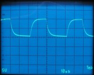
Pin 4 "OSC, Output" gave me this wave with the capacitor on:


Pin 11 "Output A" and Pin 14 "Output B" both gave me:

Pin 4 "OSC, Output" gave me this wave with the capacitor off:
-Weird, i was expecting a square wave.

I just cut a leg off the cap since i didn't felt like setting up my soldering iron now.

is pin 4 the main pin to look at? im guessing because I believe that stands for "Oscillating Output"
This is how ive been turning on the amp, with a clip connecting the remote and +12:
Here is the pinout i got from its datasheet:
I also took it out and cleaned with some Dexoit to be sure everything was connecting well.
Pin 4 "OSC, Output" gave me this wave with the capacitor on:
Pin 11 "Output A" and Pin 14 "Output B" both gave me:
Pin 4 "OSC, Output" gave me this wave with the capacitor off:
-Weird, i was expecting a square wave.
I just cut a leg off the cap since i didn't felt like setting up my soldering iron now.
is pin 4 the main pin to look at? im guessing because I believe that stands for "Oscillating Output"
Copy and paste the following list and fill in the blanks. If there is no blank space after the colon, add one between the colon and the numbers you enter. I makes it much easier to read.
DC voltage on all terminals of the SG3525
Pin 1:
Pin 2:
Pin 3:
Pin 4:
Pin 5:
Pin 6:
Pin 7:
Pin 8:
Pin 9:
Pin 10:
Pin 11:
Pin 12:
Pin 13:
Pin 14:
Pin 15:
Pin 16:
DC voltage on all terminals of the SG3525
Pin 1:
Pin 2:
Pin 3:
Pin 4:
Pin 5:
Pin 6:
Pin 7:
Pin 8:
Pin 9:
Pin 10:
Pin 11:
Pin 12:
Pin 13:
Pin 14:
Pin 15:
Pin 16:
Tested all the terminals as requested, here are my findings:
Edit: Note this was load capacitor: off
Pin 1:    0.2mV
Pin 2:    5.2V
Pin 3:    0.2mV
Pin 4:    406mV
Pin 5:    1.98V
Pin 6:    3.91V
Pin 7:    1.96V
Pin 8:    720mV
Pin 9:    6.36V
Pin 10:    3.95V
Pin 11:    6.8mV
Pin 12:    0.3mV
Pin 13:    11.2V
Pin 14:    7.6mV
Pin 15:    11.2V
Pin 16:    5.2V
Edit: Note this was load capacitor: off
Pull the SG3525 and lift pin 10 so it doesn't go back into its slot and reinsert the SG3525.
This needs to be done with no PS FETs installed.
Does that give you output pulses on the SG3525?
This needs to be done with no PS FETs installed.
Does that give you output pulses on the SG3525?
Will do,
Are these PS FETS too? they are next to the entire bank (x8) of FETS i took out. I will take them out too if so.

Also, should I check for pulses on these 3 again? 4, 11, 14

Are these PS FETS too? they are next to the entire bank (x8) of FETS i took out. I will take them out too if so.
Also, should I check for pulses on these 3 again? 4, 11, 14
I went ahead of myself and tested.
Moved pin 10 to the side:

Went ahead and tested with capacitor: off
Pin 4

Pin 11&14 now show a signal

capacitor: on
Pin 4

Pin 14

Pin 11:

although the signal is present it doesn't seem to change with or without a load.
Side note: with power on and pin 10 off, the protect light remains off, but if power is disconnected, the protect light will turn on momentarily after 5 secs
Moved pin 10 to the side:
Went ahead and tested with capacitor: off
Pin 4
Pin 11&14 now show a signal
capacitor: on
Pin 4
Pin 14
Pin 11:
although the signal is present it doesn't seem to change with or without a load.
Side note: with power on and pin 10 off, the protect light remains off, but if power is disconnected, the protect light will turn on momentarily after 5 secs
Understood, post #18 has my findings, im guessing something is not turning on the SG3525 perhaps? theoretically, if I were to put the new components back on the board while noticing this behavior, im not still out of the water yet. Maybe even burn the new MOSFETS.The load will only make a difference at the FET gate.
I'm not sure I understand. Are you saying that you had no difference on the gate pad with the 0.1uf capacitor connected across the gate/source?
I don't know why pin 10 is being driven high. You may have to follow the circuit back to see what's driving that pin.
I don't know why pin 10 is being driven high. You may have to follow the circuit back to see what's driving that pin.
- Home
- General Interest
- Car Audio
- MMats Hifi-6150D blown MOSFETs