...been working on this circuit and something to get my hands busy during vacant days. As I'm getting my grip (and brains) back with LTSpice..please let me know if what I'm doing does not involve redundant parts (and flawed results 🙂).
Closed loop.

PM/GM

Step response @ 1KHz & 20Khz


Clipping point

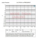
Series of Fourier test at 1Khz 1W / 20Khz 1W / 1Khz 50W / 20Khz 50W (estimated max power)


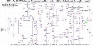
Schematic

THD may not be pleasing, I understand it is a Sziklai output..if I wanted to lower THD..H2 level goes down as well (bias current 40ma).
Let me know if the circuit will qualify as a working amp in a real world build.
Thanks!
Closed loop.
PM/GM
Step response @ 1KHz & 20Khz
Clipping point
Series of Fourier test at 1Khz 1W / 20Khz 1W / 1Khz 50W / 20Khz 50W (estimated max power)
Schematic
THD may not be pleasing, I understand it is a Sziklai output..if I wanted to lower THD..H2 level goes down as well (bias current 40ma).
Let me know if the circuit will qualify as a working amp in a real world build.
Thanks!
out of couriosity: have you tried out a bias current(sim) of 11mA?
(i have seen this in a d. self amp book..........)
(i have seen this in a d. self amp book..........)
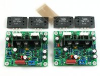
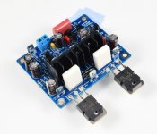
You can refer to mx50se....been working on this circuit and something to get my hands busy during vacant days. As I'm getting my grip (and brains) back with LTSpice..please let me know if what I'm doing does not involve redundant parts (and flawed results 🙂).
Closed loop.
View attachment 1073140
PM/GM
View attachment 1073141
Step response @ 1KHz & 20Khz
View attachment 1073143View attachment 1073145
Clipping pointView attachment 1073146
Series of Fourier test at 1Khz 1W / 20Khz 1W / 1Khz 50W / 20Khz 50W (estimated max power)
View attachment 1073149
View attachment 1073150
View attachment 1073151
View attachment 1073152
Schematic
View attachment 1073153
THD may not be pleasing, I understand it is a Sziklai output..if I wanted to lower THD..H2 level goes down as well (bias current 40ma).
Let me know if the circuit will qualify as a working amp in a real world build.
Thanks!
It is basically no different from your circuit. It is used by many people.
The performance test was also good.
Whether using Sanken. KEC. Or ONSEMI.
Performance has not changed.
Attachments
I did made a quick sim run between 4ma to about 15ma..output fourier result does not seem to be in optimal state, could be because I'm using faster devices? The fourier test between 30ma - 50ma shows a more linear graph.out of couriosity: have you tried out a bias current(sim) of 11mA?
(i have seen this in a d. self amp book..........)
Is this the correct schematic?You can refer to mx50se.
It is basically no different from your circuit. It is used by many people.
The performance test was also good.
Whether using Sanken. KEC. Or ONSEMI.
Performance has not changed.
The mx50se has undergone several version changes.Is this the correct schematic?View attachment 1073188
But it's basically like this.
Attachments


The small resistor will act as sensing element, supposed to be to add stability, other design had it at bases of the outputs. I've read it from other forums discussing about CFP output stability.What is the purpose of R32 and R29 ?
Very interesting. Do you have that link ?The small resistor will act as sensing element, supposed to be to add stability, other design had it at bases of the outputs. I've read it from other forums discussing about CFP output stability.
Unfortunately it has been years passed since my last diy adventure, i do believe that the emitter resistors was randomly mentioned from other topics here at DIYAudio but here's my first encounter of the said resistors. The schematic was designed by member Catalin and to my knowledge AlexMM designed a pcb for it.Very interesting. Do you have that link ?
Attachments
I actually created one design out of it and made an actual build for a test. It works fine pretty stable too but overtime, I feel like something is still missing (according to my preference of course 🙂).

Yes that was the objective, I've read from the experts that the sziklai pair is very sensitive to current imbalance, a little drift here and there and the thing will oscillate wildly...so yep I do think that was an added control?Those resistors (4.7ohm) are for correct current sharing between power transistors.
(BTW I am quoting from 'the experts' as I am a hobbyist discovering and experimenting based on the way I understood things. 😉)
Many people change circuit parameters at will.Yes that was the objective, I've read from the experts that the sziklai pair is very sensitive to current imbalance, a little drift here and there and the thing will oscillate wildly...so yep I do think that was an added control?
(BTW I am quoting from 'the experts' as I am a hobbyist discovering and experimenting based on the way I understood things. 😉)
But there is no actual measurement. In fact, sometimes measured. Not necessarily reliable.
Sometimes it takes hundreds. Thousands of people. Test on different equipment.
DIY sometimes looks simple. Very casual.
But sometimes the requirements are very high. It is even more complicated than a car.
There is no test of time. It is not a really qualified product.
^Yes Sir, thank you for your input.
Meanwhile a new idea has emerged...almost identical in simulated results with the first schematic. Except this one had higher ULGF at 1.2Mhz but with a slightly lower PM/GM. LTP current was higher in order to come up with a lower dc offset.

(I snatched member LKAs spice directive just to compare with my own results) Thanks!
Meanwhile a new idea has emerged...almost identical in simulated results with the first schematic. Except this one had higher ULGF at 1.2Mhz but with a slightly lower PM/GM. LTP current was higher in order to come up with a lower dc offset.
(I snatched member LKAs spice directive just to compare with my own results) Thanks!
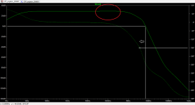
Hello again!
Can anyone help me figure out what causes this sudden boost in gain? (shown as short lifted line in the plot). I'm running out of ideas on how to fix and flatten this because I suspect 'that lift' causes the HF peaking in my square wave simulation.
Regards,
Albert

Can anyone help me figure out what causes this sudden boost in gain? (shown as short lifted line in the plot). I'm running out of ideas on how to fix and flatten this because I suspect 'that lift' causes the HF peaking in my square wave simulation.
Regards,
Albert
Hello.Hello again!
Can anyone help me figure out what causes this sudden boost in gain? (shown as short lifted line in the plot). I'm running out of ideas on how to fix and flatten this because I suspect 'that lift' causes the HF peaking in my square wave simulation.
This is due to the input two voltage amplification stages, namely, the increased input relative impedance of the second amplification stage for the RF range relative to the output of the first stage. That is, the main reason for the decrease in the output resistance of the input group of transistors due to the use of the Shiklai assembly and the Miller correction in the second stage can no longer sufficiently attenuate the signal with increasing frequency, and as a result, the loss of linearity ...
Henk.
Judging by the Bode diagram (white lines) the standard Miller correction is obtained, for high-quality comfortable sound, you need to look at the depth of Negative feedback at a frequency of 20 kHz, it cannot be arbitrarily large, nor can it be very small, in both cases there will be either an increase in dynamic distortion or growth of non-linear distortions, so this parameter should be optimal.
Attachments
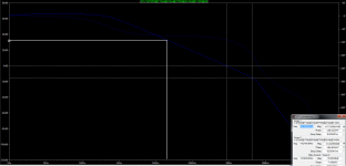
If the Bode diagram above in the topic is correct, then the gain at a frequency of 20 kHz is approximately 30-35 dB (see attach - white lines) without negative feedback, the gain of the circuit with general feedback is Ku=20Log (1 + 22 / 0.47)=33.6 dB.
That is, at a frequency of 20 kHz, there is no negative feedback at all - this contradicts high-quality sound, because the input differential stage operates at this frequency with a full input signal, and the bipolar transistor input has a very narrow section of linear work. If the entrance was on the Jfet, then in this case it would be better,, but there will be other nuances...
That is, at a frequency of 20 kHz, there is no negative feedback at all - this contradicts high-quality sound, because the input differential stage operates at this frequency with a full input signal, and the bipolar transistor input has a very narrow section of linear work. If the entrance was on the Jfet, then in this case it would be better,, but there will be other nuances...
Attachments
Henk,
That is very helpful of you, very educational from the technical point of view. This'll give me more time to 'digest' your teachings. I believe a schematic diiagram will be of much more help with my understanding...
Attached is the schematic with the bode plot in question posted from above.
Thanks!
Albert

(Ideas taken from Bigun and Bory's design).
That is very helpful of you, very educational from the technical point of view. This'll give me more time to 'digest' your teachings. I believe a schematic diiagram will be of much more help with my understanding...
Attached is the schematic with the bode plot in question posted from above.
Thanks!
Albert
(Ideas taken from Bigun and Bory's design).
- Home
- Amplifiers
- Solid State
- Another CFP output design attempt.