Hello,
As my first complete LTspice -> KiCad -> PCB manufacture project I wanted to remake my damaged driver boards for a Sansui AU-999 integrated amp from the early 70's.
I wanted to see whether there are any circuit improvements I could implement into the new PCB and I wanted to ask you guys for a bit of help in trying to achieve this.
I'm attaching the original circuit schematic for the amplifier, the F-1159 outlined circuit is the driver board I was aiming to rework.
So far, the possible improvements I have identified are:
1. Adding a Baxandall diode to the quasi-complementary output stage - could someone advise on the best location? You can see I already attempted to implement this in my schematic, I tried different configurations and this one is giving me the lowest THD figure. It was done purely by experimentation and looking at other qusi-comp circuits.
2. Changing the value of output pull-off resistors from 220R to something smaller as suggested by @steveu in another thread - The suggested 47R seems to give a good improvement in THD and helps improve the x-over distortion
3. Adding a small value resistor in series with the 15pf feedback cap - steveu also suggested adding a small resistor (100R as starting value) to the feedback cap to prevent RF from getting into the LTP input transistor
4. Adding current limiting - suggested by the same user, what and how simple it would be to implement.
5. Improving the input differential pair - this is something I wanted to investigate, would adding a current mirror/source be a simple matter with the existing configuration?
6. Adding op-amp-based DC servo - this might be too much for this project as I would need to add step-down regulators to create a dedicated bi-polar PSU rail for the op-amp to operate, I'm not sure if that would be worth the effort?
I would be grateful for any additional suggestions or help with the above,
My knowledge is still very basic but so far I've learned quite a bit from this project and I really would like to see it completed.
I'm attaching the original amplifier schematic along with my LTspice files, inc. custom libraries.
Thanks for looking into this!!
Attachments
Last edited:
Not familiar with that amp, but what you're doing will change the performance (for the better!) and may change the sound in ways you like or don't like. The THD will go down and you might find the bass is a bit thin, but more detailed and resolved. Some people don't like this, others (me) do. Use a 1N400x diode for the Baxandall, which normally goes on the drivers, not the outputs. I've pondered the same idea of adding a current source to amps like this, but never went to the trouble. Probably a good mod if you work out the details and get things at the right operating point.

I would recommend using a complementary pair, perhaps swapping the lower MJ15003 for an MJ15004, but you may like to check how well the PNP is matched to the NPN. A 1N4148 in the main current path is not going to survive the first piece of music power.
Another reason for suggesting full complementary is that triples involving both flavours of transistor (NPN-PNP-NPN) tend to be less stable,
If you prefer to keep a quasi, to improve the symmetry, I would do the following:
1. Connect the lower end of the UPPER NPN base resistor to the emitter not the centre rail.
2. Remove the lower emitter resistor of the lower NPN and reposition it between the centre rail and collector of the lower NPN.
Connect the emitter directly to the negative/ground line.
3. Add a third 47 ohm between the collector/resistor junction and the emitter of the PNP driver, and shunt it with a 1N4002 diode rather than a 1N4148.
4. Depending on whether you see any oscillatory tendency in the lower half of the output (you do have an oscilloscope, don't you?) you may need a capacitor of about 10nF across the diode too.
Alternatively, which MAY keep the configuration more stable, is to keep the upper and lower base and emitter resistors as they are, but add a third "emitter resistor" between the collector of the lower NPN and centre rail, and connect a third "base" resistor (same value, BTW, 47 ohms not 15) between the emitter of the PNP driver and centre rail, then connect the Baxandall diode between the NPN collector and PNP emitter. This increases the saturation voltage of the lower output section and could reduce peak output power slightly, but should be more symmetrical, as an alternative to the usual.
Last edited:
I have tried placing the PNP MJ15004 in place of the NPN device but I can't get it to work properly. I guess this modification will involve more than just simply replacing those parts?I would recommend using a complementary pair, perhaps swapping the lower MJ15003 for an MJ15004, but you may like to check how well the PNP is matched to the NPN.
I saw this arrangement in another circuit and it actually gave me the lowest THD figure in this amp. It must have been taken from a low-power amplifier where this arrangement was acceptable.A 1N4148 in the main current path is not going to survive the first piece of music power.
I think to keep the overall topology somehow original I would probably stick with quasi-complementary and just try to improve it.Another reason for suggesting full complementary is that triples involving both flavours of transistor (NPN-PNP-NPN) tend to be less stable,
If you prefer to keep a quasi, to improve the symmetry, I would do the following:
I'm not sure if I fully understand, do you mean (looking at my LTspice schematic) R33 to the emitter of Q10?1. Connect the lower end of the UPPER NPN base resistor to the emitter not the centre rail.
That I understand2. Remove the lower emitter resistor of the lower NPN and reposition it between the centre rail and collector of the lower NPN.
Connect the emitter directly to the negative/ground line.
Sorry, do you mean add 47ohm (with diode in parallel) between the collector-resistor junction of the lower NPN output device and the emitter PNP driver? Or resistor and diode between collector and emitter of PNP driver itself?3. Add a third 47 ohm between the collector/resistor junction and the emitter of the PNP driver, and shunt it with a 1N4002 diode rather than a 1N4148.
Yes, I do have access to an oscilloscope so I can investigate that, thanks.4. Depending on whether you see any oscillatory tendency in the lower half of the output (you do have an oscilloscope, don't you?) you may need a capacitor of about 10nF across the diode too.
That makes sense to me (I think..) I will try it once I figure out the first suggested configuration.Alternatively, which MAY keep the configuration more stable, is to keep the upper and lower base and emitter resistors as they are, but add a third "emitter resistor" between the collector of the lower NPN and centre rail, and connect a third "base" resistor (same value, BTW, 47 ohms not 15) between the emitter of the PNP driver and centre rail, then connect the Baxandall diode between the NPN collector and PNP emitter. This increases the saturation voltage of the lower output section and could reduce peak output power slightly, but should be more symmetrical, as an alternative to the usual.
Do you think improving the input diff pair will be worthwhile in this amp?
Thanks for your time John!
@john_ellis
This is the result of the secondary suggestion you made,
THD improvement is relatively small but I guess that doesn't mean much without actually performing listening tests.
I will now try to implement the first suggested mod and report back with my findings.
Thanks

This is the result of the secondary suggestion you made,
THD improvement is relatively small but I guess that doesn't mean much without actually performing listening tests.
I will now try to implement the first suggested mod and report back with my findings.
Thanks
Here's the arrangement John Linsley Hood devisedI have tried placing the PNP MJ15004 in place of the NPN device but I can't get it to work properly. I guess this modification will involve more than just simply replacing those parts?
I saw this arrangement in another circuit and it actually gave me the lowest THD figure in this amp. It must have been taken from a low-power amplifier where this arrangement was acceptable.
I think to keep the overall topology somehow original I would probably stick with quasi-complementary and just try to improve it.
I'm not sure if I fully understand, do you mean (looking at my LTspice schematic) R33 to the emitter of Q10?
That I understand
Sorry, do you mean add 47ohm (with diode in parallel) between the collector-resistor junction of the lower NPN output device and the emitter PNP driver? Or resistor and diode between collector and emitter of PNP driver itself?
Yes, I do have access to an oscilloscope so I can investigate that, thanks.
That makes sense to me (I think..) I will try it once I figure out the first suggested configuration.
Do you think improving the input diff pair will be worthwhile in this amp?
Thanks for your time John!
Attachments
Thank you for that! So I guess this illustrates what john_ellis was suggesting.Here's the arrangement John Linsley Hood devised
This arrangement takes the THD value to 0.00x ( I know real-world figure would probably be different)
(Sorry for the messy-looking schematic, I will tidy it up later)
The bias current is half the value on the neg side, I guess this will always be like that with a quasi-comp arrangement?

In post 6 - the 15 ohm should not be there in the emitter of the PNP driver, and the diode is the wrong way round.
In post 8 the lower NPN emitter resistor need not be there - it is less symmetrical keeping it as that is a cross between the two options.
When you said that the MJ15004 did not work properly, remember that you need to change the bias circuit to allow for 6 Vbe's, and with a triple output stage you may need an alternative circuit to the simple one transistor Vbe multiplier, but the arrangement in that amplifier is targetted at the rather unusual resistor load of the VAS transistor, which will give larger current variation than using a CCS.
Thanks for pointing this out, I realised about the lower NPN emitter resistor and removed it.In post 6 - the 15 ohm should not be there in the emitter of the PNP driver, and the diode is the wrong way round.
In post 8 the lower NPN emitter resistor need not be there - it is less symmetrical keeping it as that is a cross between the two options.
When you said that the MJ15004 did not work properly, remember that you need to change the bias circuit to allow for 6 Vbe's, and with a triple output stage you may need an alternative circuit to the simple one transistor Vbe multiplier, but the arrangement in that amplifier is targetted at the rather unusual resistor load of the VAS transistor, which will give larger current variation than using a CCS.
This is the final output stage configuration I settled with, I also added a current source and current mirror to the diff input stage.
All of this has lowered my THD considerably, however, I'm a bit puzzled why the input stage modification made my high-frequency performance worst than the simpler diff pair. see below
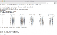
Upgraded input stage at 20kHz - high THD

Standard input stage at 20kHz - lower THD than above

Upgraded input stage at 1kHz - really good THD

Is there something in that differential pair with the current sink/mirror that is slowing the amp down hence the high THD figure?
Thanks for your time
Thanks for your reply @john_ellis,
In fact, all the operating currents are basically the same across the whole circuit.
Currents with the more elaborate input stage are matched to 4uA,
The simpler one is matched to 2uA.
Could that small difference cause such a large THD increase? The more complex input stage still performs much better at 1khz but just not as well at higher frequencies.
Any suggestions on how I could improve this?
Regards,
bias (of the output stage) is the same (+-0.5mA), set as per the original service manual at around 30mA.First thoughts - bias current the same?
In fact, all the operating currents are basically the same across the whole circuit.
Sorry John, could you clarify to me what part of the circuit am I looking at? I have 4mA going via 10k resistor R18, I can't locate the 150ohm resistor, are you referring to Q11 & Q13 emitter resistors? If so, there is no improvement in THD when they are removed. The CCS is supplying 2mA to the input stage.40V/10k=4mA, do you not need 150 ohms if you use your transistor pair for a CCS?
Check the curents by measuring the voltages across R11, R12.
Currents with the more elaborate input stage are matched to 4uA,
The simpler one is matched to 2uA.
Could that small difference cause such a large THD increase? The more complex input stage still performs much better at 1khz but just not as well at higher frequencies.
Any suggestions on how I could improve this?
Regards,
I'm slowly getting there with this project,
I still need to re-create two small replacement PCBs that will hold the rest of the passives from the output section.

I still need to re-create two small replacement PCBs that will hold the rest of the passives from the output section.
- Home
- Amplifiers
- Solid State
- Sansui AU-999 - Please help to improve Quasi-Complementary Amplifier (LTspice)