Dear all,
for the last couple of years i have read and found a lot of interesting topics about horns, hifi, amps and other interessting stuff about my hobby (and small business by now next to my full time job as an optics engineer) on this website. Finally i decided to join your community as well and i am very excited to learn and share!
Sadly i directly have to come up with a question on the Hiraga 30W Amplifier...
Short background on the history:
I am running two of those beatiful amps already, which i have build years ago with an friend of mine, who has passed away too early sadly. Now i wanted to give it another try on my own, because i am really fascinated by the sound of these amps and i wanted to learn more about electronics and i have better capabilities to manufacture nice enclosures.
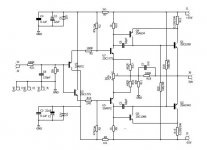
I found the PCB's on Ebay three years ago, a week ago i decided i wanted to finalize the amps already.... It's the blue ones with the little monster printed on them (no link anymore, but see pic's attached). Meanwhile i have found out, that they are very similar (but not identical) to those ones available here:
Hiraga 30W A class Amplifier - HiFiStor
But they are not completly similar, because
- the driver transistors 2SA634 and 2SC1096 are different in my kit.
The power supply came with transistors instead of diodes.
The output transistors were off as well (2SC5198 and 2SA1941 instead of 5200 and 1943)
All in all, looking back, i am afraid the ebay kit was a wierd mix of transistors and PCB's and a knock off....
The Problem:
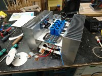
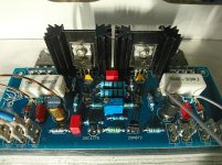
I have checked the circuit and values of resistors several times. Both channels behave similarly. My Power Supply runs at +-34V with lots of capacitors (see picture), so that should work fine.
I nevertheless only measure a very small voltage across the 0.33R resistor with 47k Resistors as R3 and R2 in place (from schematic in the link above). Putting a 200k Stereopoti in parallel allows me to increase the Voltage drop across R12/R13 (its the 0.33R ones) to around 0.2V to 0.25V (quasi cold state). Slowly lowering the resistance further, all of the sudden i can hear a "plop" and one of the two power transistors shorts and is broken (i think by then i am around 33k in total). They are attached to rather large Fischer Heatsinks (see pictures). The 300R resistor R18 looks a little brownish by now.
I have checked the 0.6mV across Q4 & Q3 and that looks fine. There is supposed to be a Voltage at R10 & R9 of around 1V (1mA@1k from the original Hiraga schematic), which seems to be a little low at my setup with around 0.65V. The zener-diodes show 22.0V, as supposed to be.
I am thinking that my transistors 2SA940 and 2SC2073 do not fit well as the drivers. The datasheets are hard to compare (for me and my limited knowledge/experience) because the data given does not match (Voltages and currents where the Data is given varies, see attached pdfs).
So my question now is:
Can anyone help me to find out what goes wrong here?
Is it worth changing the drivers to the 634/1096 ones?
Might it be a problem of matching the input transistors?
Waht am i overlooking, because the problem occurs in both channels?
How can i systematically track the error (i do not know which voltages should be where without simulation the circuit?)
I am a little lost beacuse i am in the wierd state of generally understanding how a transistor works, but still beeing (massively 😉 ) overwhelmed with analyzing schematics to great detail. And then there are three versions of this amp (my old one, the ebay one which is the problem, the linked one) with different transistors and resistorvalues, which dont make it easier to truly understand the important parts of the circuit.
Sorry for the long story and thanks a lot for your support!
For a better understanding i have attached a few pictures of the amplifer.
for the last couple of years i have read and found a lot of interesting topics about horns, hifi, amps and other interessting stuff about my hobby (and small business by now next to my full time job as an optics engineer) on this website. Finally i decided to join your community as well and i am very excited to learn and share!
Sadly i directly have to come up with a question on the Hiraga 30W Amplifier...
Short background on the history:
I am running two of those beatiful amps already, which i have build years ago with an friend of mine, who has passed away too early sadly. Now i wanted to give it another try on my own, because i am really fascinated by the sound of these amps and i wanted to learn more about electronics and i have better capabilities to manufacture nice enclosures.
I found the PCB's on Ebay three years ago, a week ago i decided i wanted to finalize the amps already.... It's the blue ones with the little monster printed on them (no link anymore, but see pic's attached). Meanwhile i have found out, that they are very similar (but not identical) to those ones available here:
Hiraga 30W A class Amplifier - HiFiStor
But they are not completly similar, because
- the driver transistors 2SA634 and 2SC1096 are different in my kit.
The power supply came with transistors instead of diodes.
The output transistors were off as well (2SC5198 and 2SA1941 instead of 5200 and 1943)
All in all, looking back, i am afraid the ebay kit was a wierd mix of transistors and PCB's and a knock off....
The Problem:
I have checked the circuit and values of resistors several times. Both channels behave similarly. My Power Supply runs at +-34V with lots of capacitors (see picture), so that should work fine.
I nevertheless only measure a very small voltage across the 0.33R resistor with 47k Resistors as R3 and R2 in place (from schematic in the link above). Putting a 200k Stereopoti in parallel allows me to increase the Voltage drop across R12/R13 (its the 0.33R ones) to around 0.2V to 0.25V (quasi cold state). Slowly lowering the resistance further, all of the sudden i can hear a "plop" and one of the two power transistors shorts and is broken (i think by then i am around 33k in total). They are attached to rather large Fischer Heatsinks (see pictures). The 300R resistor R18 looks a little brownish by now.
I have checked the 0.6mV across Q4 & Q3 and that looks fine. There is supposed to be a Voltage at R10 & R9 of around 1V (1mA@1k from the original Hiraga schematic), which seems to be a little low at my setup with around 0.65V. The zener-diodes show 22.0V, as supposed to be.
I am thinking that my transistors 2SA940 and 2SC2073 do not fit well as the drivers. The datasheets are hard to compare (for me and my limited knowledge/experience) because the data given does not match (Voltages and currents where the Data is given varies, see attached pdfs).
So my question now is:
Can anyone help me to find out what goes wrong here?
Is it worth changing the drivers to the 634/1096 ones?
Might it be a problem of matching the input transistors?
Waht am i overlooking, because the problem occurs in both channels?
How can i systematically track the error (i do not know which voltages should be where without simulation the circuit?)
I am a little lost beacuse i am in the wierd state of generally understanding how a transistor works, but still beeing (massively 😉 ) overwhelmed with analyzing schematics to great detail. And then there are three versions of this amp (my old one, the ebay one which is the problem, the linked one) with different transistors and resistorvalues, which dont make it easier to truly understand the important parts of the circuit.
Sorry for the long story and thanks a lot for your support!
For a better understanding i have attached a few pictures of the amplifer.
Attachments
200mV across a 0.33R.
That is a lot of wasted power to dissipate. 600mA quiescent current will kill any transistor that is not kept cool.
That is a lot of wasted power to dissipate. 600mA quiescent current will kill any transistor that is not kept cool.
The original transistors were lower voltage. 30 volts Collector to emitter
But were much higher in speed around 55 Mhz
The website mentioned changing the drivers to run the amplifier on higher voltage.
much higher voltage 150 volt Collector to emitter.
They are rather slow actually around 4 Mhz
So any stabilization compensation capacitors might need to be a different value for such
a slow transistor. not much different than MJE340/350 which is common but pitiful slow transistor as well.
Curious if the amp is even stable.
Im not sure if there is much benefit to over bias the amplifier so much.
600 ma of idle current wont do much for such slow drivers.
This amp could just run around 30 to 50 ma.
Just a overbiased class A/B amplifier.
Good replacement driver would only need to be in the 60 to 80 volt range with 35 volt power rails
and something that would would be closer to the original Toshiba transition speed of 55 Mhz.
Last edited:
Good idea to set the DC offset first
the offset tends to sit negative when ideal
Bias will rise when offset is set right
and everything warms up.
The 47K resistors are to high to get bias up to 600ma
They only need to be lowered to around 39K.
If the drivers are a T0-220 package
Common used MJE packages from OnSemi
MJE15028/ 15029
MJE15030/ 15031
most likely all updated to PB free
so when you search for those parts they will usually have
a G suffix at the end. MJE15028G / MJE15029G
Last edited:
Hi there,
let me comment on your posts.
@JonSnell Electronic: As far as i understood, this amp (transistorchoice/cooling/supply etc.) is designed to work at raher high bias currents to reach class A state. I am using proper cooling, so i think it should be possible to run the amp at high currents and my problem originates from somewhere else. Please correct me if any
@White Dragon: Thanks for the comments. Let me sum it up, i will:
- check for oscillations
- set 47k to rather 39k (supports my findings so far)
- check and adjust DC-offset (in a state with rather low bias-current), readjust when warmed up
- let it heat up properly to see which current levels are showing up with increasing temperature
- change drivers to one of the mentioned pair (high rail voltages, high frequency capabilities)
Thanks a lot for your ideas so far, i will let you know any results!
Tobi
Hi there,
so i have some news for you after i have tried a few things at the workshop today. Thanks for your ideas, they helped!
1) First and foremost: The amp is running. 🙂
2) I have replaced the 47k with 33k and after 30minutes i have approx. 250mV across the 0.33R resistor. I feel that is still too little, because the heat sinks are barely getting warm 😉. Might that situation change with the new drivers (MJE15030/ 15031)? I guess lowering the 33k even more is not a good idea, because then the power transistors immediately die... So how could i get more bias current? Will it get "more class A" then (with higer bias?)? Sorry if the questions are stupid, a just know that my other Hiraga runs way hotter and i dont want to "loose" sonic quality...
3) One side shows 250mV, the other more like 180mV across 0.33R. Might that be due to some variations in the 0.33k resistors? Would that be more equal with better matched resistors or do rather the transistors have to be matched for that?
4) I send a square wave (1kHz, 50% duty cycle) into the amp but measured rather a square wave with some decaying top and bottoms (like the RC charging curves of a capacitor). (My cellphone died, so no pics, sorry!) The sound is nice though, so i am wondering where this behavior is coming from and why it is not visible with sine waves. (i know that square waves need a lot (especially high) of fourier frequencies if shown in k space, so that's why a change in square-waveform should show high frequency behavior and transitional response. Nevertheleess i would have expected a sonic difference with such a massive change in waveform. Maybe i'll check my oscilloscope these days.
5) I checked for oscillations but there were non, as far as i could check
So for now i think i will be listening to the amp a little bit longer and try to understand which effect is caused by which part of the circuit. In case you have some ideas or comments on the effects above i'd be happy to know.
Have a great evening,
Tobi

Hi, you still have the Hiraga? I have played on a Hiraga 30W now for 4 years. I have never measured the bias. The heatsink is big an the temp was 50-55 degree C. Now I have instaled Hiraga 30W with kobuta reg. I measure 0.4V ( 400mV ) across 0.33 Ohm. That give around 1.0A ( class A up to 10W ). Jims Audio told that to me. But heatsink are runing cold. But it sound nice. But knowing the bias is a bit low can fast keep you awake at nights ( :
Frank
Frank
+/-34V supply is suitable for a 70W amplifier. For class-A that means about 3 sets of power transistors per channel. For a 30W amp, you need a power supply not more than +/-24VDC.
Looking at the schematic, your problems are to be expected. The input section has been successful in other amps, but the output is just crude and unpredictable.
Beware that a "beautiful" schematic does not make a good amplifier. Remember that the power ratings of transistors are based on the virtually impossible condition of Tc=25C. The actual safe dissipation is something less than half that. A Class-A amp should be easy, provided you do the thermal math (and SOA), and the idle current is well controlled.
On my first Hiraga build in the 80s, I went a little hot on Vcc and bias. The poor transistors did not survive, despite the big heat sinks. Be careful!
Oh you are so wrong you have nooooo idea. But that's OK if you haven't used one. 😉Beware that a "beautiful" schematic does not make a good amplifier.
There are only a few transistor amps i like to listen to and that is one of them... (le Monstre included)
Dear all,
i just found out, that there are new posts in this thread. Let me quickly answer to some of those:
@Sagen Yes. I do still have my amplifiers and i like them very much. Indeed i want to learn more about Class-A amps and going for some PASS-DIY and Hiraga 7W amps now as well. I am happy to hear that you measure the proper bias current. Which heatsinks do you have? Maybe they are so big that they just stay cool? Are you saying, that after using the kobuta regulation they tend to stay cold? Maybe you loose some voltage (common for regulators) and thus have a lower biasing now?
@steveu As far as i know and can see from the schmeatics, the amp is meant to be run at +-35Volts. Are you calculating U^2/R = 150Watts @8Ohms and going for 50% Efficiency? --> Approx 70Watts? The thermal math was done carefully, that is not the issue. But i will check, any voltages that might occur too high for the transistor specs once again. Thnaks for the hint! Can you explain what you mean with "the output stage is crude"? That amp is built very minimalistic and without a lot of stabilizing measures, you are right. But as far as i know, that was known and done for sonic anhancements?
@Pano Yeah, ill be careful. Nevertheless, I have some spare transistors on stock already 😉 The heatsink is not the problem i think. It pops so fast, that i expect voltages (or base currents) beeing too high at some point because of an unlucky combination of driver transistors / resitors. But i'll go into depth in the upcoming weeks 🙂
Kind regards, Tobi
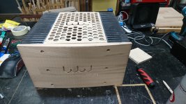
PS: This will be the new enclosure for the 7W Version. The amp i have built years ago but with limited resources and now i want to set it up nicely 🙂

i just found out, that there are new posts in this thread. Let me quickly answer to some of those:
@Sagen Yes. I do still have my amplifiers and i like them very much. Indeed i want to learn more about Class-A amps and going for some PASS-DIY and Hiraga 7W amps now as well. I am happy to hear that you measure the proper bias current. Which heatsinks do you have? Maybe they are so big that they just stay cool? Are you saying, that after using the kobuta regulation they tend to stay cold? Maybe you loose some voltage (common for regulators) and thus have a lower biasing now?
@steveu As far as i know and can see from the schmeatics, the amp is meant to be run at +-35Volts. Are you calculating U^2/R = 150Watts @8Ohms and going for 50% Efficiency? --> Approx 70Watts? The thermal math was done carefully, that is not the issue. But i will check, any voltages that might occur too high for the transistor specs once again. Thnaks for the hint! Can you explain what you mean with "the output stage is crude"? That amp is built very minimalistic and without a lot of stabilizing measures, you are right. But as far as i know, that was known and done for sonic anhancements?
@Pano Yeah, ill be careful. Nevertheless, I have some spare transistors on stock already 😉 The heatsink is not the problem i think. It pops so fast, that i expect voltages (or base currents) beeing too high at some point because of an unlucky combination of driver transistors / resitors. But i'll go into depth in the upcoming weeks 🙂
Kind regards, Tobi
PS: This will be the new enclosure for the 7W Version. The amp i have built years ago but with limited resources and now i want to set it up nicely 🙂
TobiK: I have heatsink from Webra in Sweden. W-209mm + H-75mm and L-200mm. C/W = 0.033.
Im not sure by the bias thing, measure 401mV over 0.33 so 1.2A. Still running cool, 20 degree down from oem 30W ( bias at around 1.4A ).
Frank
Im not sure by the bias thing, measure 401mV over 0.33 so 1.2A. Still running cool, 20 degree down from oem 30W ( bias at around 1.4A ).
Frank
Most important: differ "Single Ended" and "Push Pull".... i want to learn more about Class-A amps...
PP is, strictly speaking, two audible different amplifiers, often driven by twi audible different psus: does differ the signal into two halfwaves and modulate the halfwaves audible different, by audible different components:
less cleanness, or: more uncleanness;-)-;
Dear,Dear all,
for the last couple of years i have read and found a lot of interesting topics about horns, hifi, amps and other interessting stuff about my hobby (and small business by now next to my full time job as an optics engineer) on this website. Finally i decided to join your community as well and i am very excited to learn and share!
Sadly i directly have to come up with a question on the Hiraga 30W Amplifier...
Short background on the history:
I am running two of those beatiful amps already, which i have build years ago with an friend of mine, who has passed away too early sadly. Now i wanted to give it another try on my own, because i am really fascinated by the sound of these amps and i wanted to learn more about electronics and i have better capabilities to manufacture nice enclosures.
I found the PCB's on Ebay three years ago, a week ago i decided i wanted to finalize the amps already.... It's the blue ones with the little monster printed on them (no link anymore, but see pic's attached). Meanwhile i have found out, that they are very similar (but not identical) to those ones available here:
Hiraga 30W A class Amplifier - HiFiStor
But they are not completly similar, because
- the driver transistors 2SA634 and 2SC1096 are different in my kit.
The power supply came with transistors instead of diodes.
The output transistors were off as well (2SC5198 and 2SA1941 instead of 5200 and 1943)
All in all, looking back, i am afraid the ebay kit was a wierd mix of transistors and PCB's and a knock off....
The Problem:
I have checked the circuit and values of resistors several times. Both channels behave similarly. My Power Supply runs at +-34V with lots of capacitors (see picture), so that should work fine.
I nevertheless only measure a very small voltage across the 0.33R resistor with 47k Resistors as R3 and R2 in place (from schematic in the link above). Putting a 200k Stereopoti in parallel allows me to increase the Voltage drop across R12/R13 (its the 0.33R ones) to around 0.2V to 0.25V (quasi cold state). Slowly lowering the resistance further, all of the sudden i can hear a "plop" and one of the two power transistors shorts and is broken (i think by then i am around 33k in total). They are attached to rather large Fischer Heatsinks (see pictures). The 300R resistor R18 looks a little brownish by now.
I have checked the 0.6mV across Q4 & Q3 and that looks fine. There is supposed to be a Voltage at R10 & R9 of around 1V (1mA@1k from the original Hiraga schematic), which seems to be a little low at my setup with around 0.65V. The zener-diodes show 22.0V, as supposed to be.
I am thinking that my transistors 2SA940 and 2SC2073 do not fit well as the drivers. The datasheets are hard to compare (for me and my limited knowledge/experience) because the data given does not match (Voltages and currents where the Data is given varies, see attached pdfs).
So my question now is:
Can anyone help me to find out what goes wrong here?
Is it worth changing the drivers to the 634/1096 ones?
Might it be a problem of matching the input transistors?
Waht am i overlooking, because the problem occurs in both channels?
How can i systematically track the error (i do not know which voltages should be where without simulation the circuit?)
I am a little lost beacuse i am in the wierd state of generally understanding how a transistor works, but still beeing (massively 😉 ) overwhelmed with analyzing schematics to great detail. And then there are three versions of this amp (my old one, the ebay one which is the problem, the linked one) with different transistors and resistorvalues, which dont make it easier to truly understand the important parts of the circuit.
Sorry for the long story and thanks a lot for your support!
For a better understanding i have attached a few pictures of the amplifer.
I read your message right today (09-06-2023). I made this amplifier around 6 months back. I used TIP41C and TIP42C as Driver and TIP35C and TIP36C as Output (You can use 2SC5200 and 2SA1943 at the output stage). input transistors and other components are the same as per your schematic. 47K/1W resistors are changed to 33K/1W to adjust the quiescent current. Power Supply is +/- 35VDC. before adjusting trim pot (500E) short input points. Try to use input transistors with the same hfe.
- Home
- Amplifiers
- Solid State
- Hiraga 30W Transistors failing at 200mV bias current