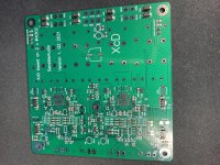
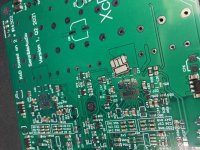
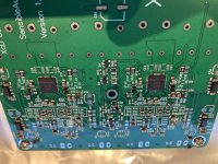
Have gotten some boards made for a 4 channel amp based on IR4302.
JLCPCB do not stock IR4302 so could unfortunately not get these mounted.
So have purchased some chips and I'm ready to try mu luck.
But how to best go about it 😕
I do not have a stensil for the IC so can't just use that and some reflow solder paste.
The PCB is HASL - Hot Air Solder Leveling, treated from manufactory.
Of course step 1 is to thoroughly clean both pcb and chip with Isopropyl alcohol.
I could give the inner pads, the large ones a very thin layer of solder paste, with a toothpick or something.
I could then apply all other pads with liquid solder flux.
Should I also flux the chip?
Placing the chip as precise as possible and apply heat with a hot air solder gun.
Will the chip move into place by it self??
I'm thinking that soldering the small outer pads with a pointed solder iron after is the way to go ??
Any good suggestions, by some with real experience in soldering items like this??
I'm used to solder components down to 0603, MS8, TSSOP, SOP etc.
Thanks in advance and kind regards Baldin
Attachments
I soldered similar pieces but from an already used pcb, say, repairing, but never from new. In my experience, warm the pcb and the chip using as few temperature as you can. I don't recomend pb free because of higher fusing temp and also it breaks easily.
Respect to the flux, I suggest to use a white past similar to wax, but I don't know how it is called in English. Then, let the pcb to cool and clean the flux carefully with proper solvent (we used MEK here). Check with a vom if there are shorts under the device prior to solder orher pieces less difficult. Also use good light and a magnif. glass if needed.
Respect to the flux, I suggest to use a white past similar to wax, but I don't know how it is called in English. Then, let the pcb to cool and clean the flux carefully with proper solvent (we used MEK here). Check with a vom if there are shorts under the device prior to solder orher pieces less difficult. Also use good light and a magnif. glass if needed.
Hi Osvaldo
Yes I also swear to old pb solder ... I still have a roll of thin Weller (I think it is) solder with 2% silver ... don´t know what I'll do when it finally runs out ... best stuff ever 😉
Weller has some WAX flux .... that kind?
Weller soldering pastes, WEL.LF25 |EN|
... Rasin based
What about the idea to only solder the middle part first??
Surface mount rework needs lots of flux, a bath of it is the correct amount!, you can't tolerate anything oxidizing. Rosin flux for electronics is the sort to get, never ever anything designed for plumbing or brazing (!!!!!)
If you’re unused to it, solder rather that hot air… but
Unless you’re gonna omit the hidden lands for heat sinking (not that good an idea), you’re gonna need a good preclean and board preheating , and attention to getting those hidden lands flowed first (and the chip aligned of course) , forget the pins til you’ve got the chip stuck down on the hidden lands
Unless you’re gonna omit the hidden lands for heat sinking (not that good an idea), you’re gonna need a good preclean and board preheating , and attention to getting those hidden lands flowed first (and the chip aligned of course) , forget the pins til you’ve got the chip stuck down on the hidden lands
Take it to a mobile repair shop, they do this all the time.
Just tell them how it is to be oriented.
Just tell them how it is to be oriented.
Yeah, I used something similar to this. The main advantage is that it evaporates easily giving no rests under the device/pcb gap. Also resin based fluxes may cause damage by electrolysis and in rf parts, it has large capacitance constant (dielectric) and looses (conductance).
I flux paste the pins and beneath the IC.
Place chip pins "exactly" on pads.
Dab of solder on the iron and tack one side very carefully without moving the IC.
I then drag solder with not too much solder on the iron along the pins/pads.
If there are shorts loads of flux paste and no solder on iron drag shorts away from pin.
If all else fails copper braid will remove stubborn shorts.
Then check with a x10 magnifying glass there are no shorts.
I have done 0.5 mm pads with 100 pins with this method loads of times.
Rarely get a failure now.
And use decent leaded solder, I bought in some chinese stuff and all it would do was blob and barely melt. Couldnt get IC back off so had to bin the pcb.
Here goes nothing!
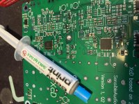
Got some new solder paste from a shop in Copenhagen ... yes a real shop 😉 ...
Cleaned surfaces and put some paste on the inner pads.
Placed as good as I could .... man would be nice with a microscope
A it hard to place as it did not really stick well. I used a quite limited amount of paste not to make any shorts ...
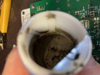
Used a hot air gun like this:
SMD loddestation - WEP 858D - 700W
- Matronics
Tried to follow a reflow profile, heating up to 160 deg for ca 2½ min, further to 250 deg for ca 1 min, and then slowly cooling down over ca 1 min
Will take it to work on Monday to check that the alignment is spot on inspecting with a microscope, before I solder the other pads!
Is this a difficult soldering ... I bet ya 😉
Got some new solder paste from a shop in Copenhagen ... yes a real shop 😉 ...
Cleaned surfaces and put some paste on the inner pads.
Placed as good as I could .... man would be nice with a microscope
A it hard to place as it did not really stick well. I used a quite limited amount of paste not to make any shorts ...
Used a hot air gun like this:
SMD loddestation - WEP 858D - 700W
- Matronics
Tried to follow a reflow profile, heating up to 160 deg for ca 2½ min, further to 250 deg for ca 1 min, and then slowly cooling down over ca 1 min
Will take it to work on Monday to check that the alignment is spot on inspecting with a microscope, before I solder the other pads!
Is this a difficult soldering ... I bet ya 😉
Attachments

Hmmm did a small test with a multimeter .... short btw Vss and one output ... :| .... dmn .... do it again ......
Another attempt, and realizing that the other chip is not soldered well at all either. The paste has jus dried and have thereby glued it together a bit.
Off we go, and try again.
But I simply can not get enough heat under the chip. Tried to heat the board up from underneath before heating from the top, but no chance.
What is not helping is that the pads underneath is used for heatsinking, and the board seem to work quite well for this .... but also therefor transferring the heat elsewhere!
And modern Pb free solder paste is no help at all either .... flows really bad even if you just heat it with a soldering iron!
Beginning to think I stand a better chance with using old solder and just applying to the pins.
With enough good flux I might get it to flow in under the chip?!?!?
In the next design I think I will make one of the vias larger and not tented.
Then I could solder the pins first and then solder the inner pads from the other side?!
You need a stencil and oven really for this kind of chip. For rework with power pads you have to heat the board quite a lot on the underside ideally. Or use a good refractory tile underneath and take your time for the board to heat through - using the largest air nozzle.
Lots of flux is a given - a lake of it is essential for rework.
Lots of flux is a given - a lake of it is essential for rework.
Not sure this is the best advice, but here are some thoughts based upon a BGA rework I did at home a couple of times:
Do you have a hot plate and a thermocouple?
In a pinch I used a single burner (smooth top) electric cooking top and copper/aluminum blocks to bring the (pre)heat to the bottom thermal vias of the PCB. Then I add heat to the top with a heat gun. I think the thermocouple and kapton tape is a must to make sure the PCB is a reasonable temperature.
The mobile repair shop sounds like a good idea. Without the right tools you can end up cooking/damaging parts.
The mobile shop would have fresh consumables and the right equipment, also experience, which is what really counts, in these fine pitch jobs sometimes an occasional dabbler will not be able to do the proper job.
We have a client who had to attach 64 pin SMD to the PCB, 20 years back.They tinned the PCB, and the chips, then soldered the corner pins. Then used plenty of flux, a ceramic tip fine iron, and braid to finish.
Those were OEM chips from Japan for glucometers, and they had to stop production as the chips stopped coming, the bigger customer leaned on the chip supplier.
Thanks for your input 🙂
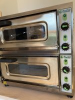
Been thinking about using an oven .. well actually 2.
I'm blessed with a real pizza oven with 2 shelves ..... highly recommended for those Friday nights 🙂 ... but that´s another story 😀
One like this: ELECTRIC PIZZA OVEN MICROV2C - Fimar
I can regulate the temperature independently in both ovens and both for the plate and the upper temp.
I was thinking of using one as a preheater on 150 deg C, and the second on 220-250 deg C.
Then put the board in at 150 for 3 min, and then switch to the other oven for 250 deg C for 2 min, and then out ...
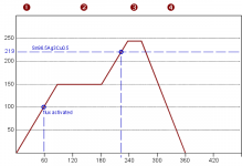
It would sort of mimic a reflow profile like the attached.
I would place the pcb on a piece of alu foil to protect my beloved ovens.
It will of course reflow the other components, but think that will be ok.
Yes I'm missing a stensil ... but will have to do with a tooth pick a careful amounts of paste
Been thinking about using an oven .. well actually 2.
I'm blessed with a real pizza oven with 2 shelves ..... highly recommended for those Friday nights 🙂 ... but that´s another story 😀
One like this: ELECTRIC PIZZA OVEN MICROV2C - Fimar
I can regulate the temperature independently in both ovens and both for the plate and the upper temp.
I was thinking of using one as a preheater on 150 deg C, and the second on 220-250 deg C.
Then put the board in at 150 for 3 min, and then switch to the other oven for 250 deg C for 2 min, and then out ...
It would sort of mimic a reflow profile like the attached.
I would place the pcb on a piece of alu foil to protect my beloved ovens.
It will of course reflow the other components, but think that will be ok.
Yes I'm missing a stensil ... but will have to do with a tooth pick a careful amounts of paste
Attachments
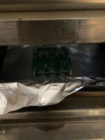
Ok, has taken a while ..... maybe mostly to take on the chance of baking the board in the oven .... but here goes.
I set the lower oven to 150 deg, and the upper to 250 degree.
Gave the board 6 min at 150 and 2 min at 260 degree, took the board out for immediate cooling.
I only applied solder paste to the inner pads.
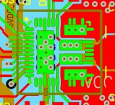
So next step is securing that no pads are soldered together. Will do that with a simple ohm meter. Layout around the IR chips as last picture.
Then soldering of all leads, and then checking with the ohm meter again.
Final step is to mount the rest of the components and hold ones breaths and cross the fingers ...... let's see whan that'll be 🙂
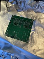
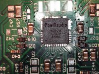
The close up of the chip is with my new microscope 😉 .....
I set the lower oven to 150 deg, and the upper to 250 degree.
Gave the board 6 min at 150 and 2 min at 260 degree, took the board out for immediate cooling.
I only applied solder paste to the inner pads.
So next step is securing that no pads are soldered together. Will do that with a simple ohm meter. Layout around the IR chips as last picture.
Then soldering of all leads, and then checking with the ohm meter again.
Final step is to mount the rest of the components and hold ones breaths and cross the fingers ...... let's see whan that'll be 🙂
The close up of the chip is with my new microscope 😉 .....
Attachments
- Home
- Design & Build
- Construction Tips
- Soldering IR4302 by hand .... anyone tried??