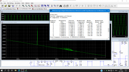
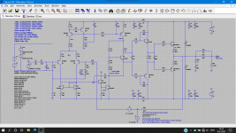
I tried the blameless circuit with inexpensive and easy-to-find components in my place of residence. Results like this. How to raise a slew rate. You can also advise and repair this series
Attachments
Why increase the slew rate? You'd be hard pressed to find an audio signal with more than a few V/µs that didn't fry your tweeters! 100W into 8 ohms at 30kHz is only 5V/µs
Dear Mark Tillotson
Thanks for the advice. I want to develop this circuit next to the power reaches 300 watts. Now still considered for loads (VAS) with large currents and gains in the LTP with high slew rate and smaller distortion
Thanks for the advice. I want to develop this circuit next to the power reaches 300 watts. Now still considered for loads (VAS) with large currents and gains in the LTP with high slew rate and smaller distortion
" I want to develop this circuit next to the power reaches 300 watts" -
Other architecture of the output stage. At least several pairs of output transistors in parallel.
Other architecture of the output stage. At least several pairs of output transistors in parallel.
I tried the blameless circuit with inexpensive and easy-to-find components in my place of residence. Results like this. How to raise a slew rate. You can also advise and repair this series
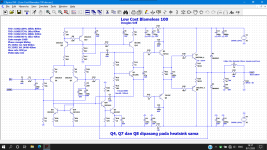
You should re-consider the effect of adding R28 (10k) into the series connection of Q16 to ground. This changes the function for the latter from an emitter follower to an inverting amplifier stage. Any capacitance between the collector and base will be amplified and presented as a load to be driven at Q16 base.
This load will also be non-linear since the capacitance at Q16 is inversely proportionate to the square root of the voltage applied to the collector. This will vary with the current passing via R28.
When the collector voltage is low the collector base capacitance will be high (0 Volts is high with respect to negative supply values) and at the same time the width of the base will expand resulting in a loss of gain - due to base width modulation - for more detail search for articles on Early Effect.
I have seen an instance like R28 have been included where instability has resulted. This could be mitigated by adding a capacitor in parallel but with the complexity of this circuit there can be no guarantees.
Why are you using old slow TIP41 & 42 for drivers, which are 10x slower than the ~5200 outputs? Drivers should be 40MHz parts min. And the base stoppers and driver CB caps are probably a bad idea; use only if you have to, but they could also create stability problems.
The R28 thing just needs a decoupling cap, maybe. Removing it leads to other problems, including excessive VAS currents on clipping. The VAS is wrapped in the C7 compensation cap so minor delays from a fast Q16 are completely buried.
R35+C9 is not a good idea. If you are worried about TIM then increase the LTP degeneration. Faster drivers would probably make this unnecessary.
R18+C23 also a poor choice. The VAS needs a diode to keep it from saturating.
The Zobel network C18+R31 should not be necessary for this 2EF output configuration.
R30 and R34 should be about 100 ohms so that Q11 doesn't saturate.
I would not build anything of any size without a current limit. Otherwise one momentary whoops and it blows up in an instant.
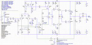
Thanks yours correction. Now i try to fix it problems. For opimize driver transistor capability. I try using 2SC4793 (pair) or 2SC5171(pair). For R28 i try remove it and connect to GND directly. Lead compensation i try to leave it.
If you remove R28 then increase R41 to 2k2 so the impedance seen by Q1 will be higher.
In the case I mentioned in post 5 the value of the equivalent R41 had also been reduced which had a negative impact on the equivalent to Q3 - forcing too much current into the base makes matters worse - transistors can saturate.
In the case I mentioned in post 5 the value of the equivalent R41 had also been reduced which had a negative impact on the equivalent to Q3 - forcing too much current into the base makes matters worse - transistors can saturate.
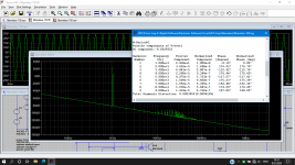
This is the result of changes with suggestions you guys. Many improvements however there is a decrease in at the slew rate. Maybe what I did
Attachments

Last edited:
Use transistor driver with high fT you can remove capacitor on basis-collector of transistor driver. Increase LTP current. Add Miller input inclusive compensation (capacitor from VAS collector to inverting input) to reduce Miller capacitor on VAS or you can use transitional miller compensation.
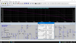
Thanks for best information. Today i compare miller and lead compesation with huge improvement up to 40uS. But when use TMC (Transitional miller compesation) i face problems with gain and phase margin. How to apply TMC in this circuit. Thanks sir
Dear Mark Tillotson
Thanks for the advice. I want to develop this circuit next to the power reaches 300 watts. Now still considered for loads (VAS) with large currents and gains in the LTP with high slew rate and smaller distortion
In that case I'll second the advice - higher voltage transistors may be needed, more current in the input pair and the VAS (so more heatsinking, different transistors perhaps). Output devices will need to be more robust to voltage and secondary breakdown, and more current handling (more pairs).
The higher the power the more important protection circuitry becomes, such as SOA protection.
Increasing power levels makes it harder to get lower distortion as you have less choice of components, though cascoding some of the devices may give more options.
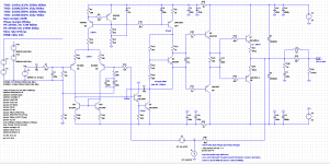
Problem resolved. I raise the LTP degeneration and current LTP and leave some components. With very significant results. Thank you very much everything. Hopefully your day is good
Attachments

Last edited:
Try thinking of Q15 as a common emitter amplifier with a bootstrapped collector load due the inclusion of C3.
I read the book and built the Load Invariant Blameless amp. 1. The book goes into each amplifier stage in great detail. Pouring over that to select new devices would be where I would start. 2. An automated regression test suite that you can run on your LTspice model after each change that would produce a small list of numeric results that you could log and quickly compare against the initial design will help you avoid running too far down dead ends. As the model is ascii text and spice can be run from a command line, any scripting language can be used to run a set of predefined analysis sequentially.
RC filter.[/QUOTE
The a.c. output of a common emitter amplifier is inverted with respect to a.c. applied either at the emitter or the base.
We have a common emitter amplifier here with C3 providing a.c. negative feedback from the split (bootstrapped) collector load to the emitter.
This is a case of active versus passive filtering.
.......perhaps a ccs with filter cap?
D. Self "audio power amplifier design handbook" fifth edition, chapter 4, page 101 at the bottom gives a hint..........
D. Self "audio power amplifier design handbook" fifth edition, chapter 4, page 101 at the bottom gives a hint..........
Yes the CCS shared for LTP and VAS. Schematic by Douglas Self handbook. The one of various method to create harmonics profile and CCS variation like diode biasing (Dx Blame), led biasing, zener regulation etc
Last edited:
- Home
- Amplifiers
- Solid State
- Low Cost Blameless 100