Zener designated ZD1 on the main board is shorted.
Best I can make out is 1N739A.
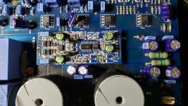
There are 2 of these zeners servicing the output driver board it looks like.
Best I can make out is 1N739A.
There are 2 of these zeners servicing the output driver board it looks like.
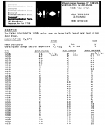
ZD1 and ZD2 should be the same. Could it be a 1N4739A? It could be the 9v regulator for the driver board.
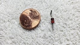
I guess that would make more sense than the 1N739A at 110V. Are there any trick to reading glass diodes. Its very hard to tell that numbers are there at all.
Is the problem that they're not printed well or that it's too small to see?
If you have a supply that's capable of producing more voltage than the Zener, you can insert a 1k resistor (starting point) in series with the Zener and increase the voltage across the resistor/Zener until you see where the voltage across the Zener stops increasing.
If you have a supply that's capable of producing more voltage than the Zener, you can insert a 1k resistor (starting point) in series with the Zener and increase the voltage across the resistor/Zener until you see where the voltage across the Zener stops increasing.
Too small to see.
Should I be able to read the DC voltage of the zener regulator on the non-grounded side of the zener? There is +12 into the 33 ohm resistor on one regulator and -12 on the other 33 ohm. On the regulated side there is less than .5V. These regs service the IC's on the output driver board. Could they be bad and are loading the regulator.
Should I be able to read the DC voltage of the zener regulator on the non-grounded side of the zener? There is +12 into the 33 ohm resistor on one regulator and -12 on the other 33 ohm. On the regulated side there is less than .5V. These regs service the IC's on the output driver board. Could they be bad and are loading the regulator.
If you're in the US, a 'DrMon otoscope' (walmart) is a great lighted magnifying glass.
You measure directly across the legs of the zener diode. Do not power up the amp with any Zener diode out of the circuit.
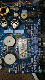
It's possible that something on the driver board or on the main board (shorted cap) could be pulling the voltage down. Photos or at least circuit board designations would be very helpful.
You measure directly across the legs of the zener diode. Do not power up the amp with any Zener diode out of the circuit.
It's possible that something on the driver board or on the main board (shorted cap) could be pulling the voltage down. Photos or at least circuit board designations would be very helpful.
The driver board was in backwards.
I could not figure out why the +9.1 from the + zener regulator was going to the negative V pin on the IC's.
I pulled the driver board and surprise the board pinout was underneath where you couldn't see it.
After pulling board the zener supplies 9.1V +/- are stable. You were correct on suggesting the 1N4739A as it turns out.
Now if I set the board back in correctly the IC's are stable on the -9.1V pin but the V+ pin is probing -5.7V. And the output at the +9.1V zener is drawn down to +8V. Not sure if it is a great connection as I have not soldered the header pins on the driver board.
Possible that the reverse polarity on the IC's damaged them? All other components on the driver board are checking ok.
Attachments
That is where my troubleshooting started in that I was trying to figure out why I had wrong voltages on the driver board IC's. I traced it back to the shorted zener. Now that the zener's have been replace and the board is in properly (although not soldered) I am probing the V+ and V- pins on the driver board IC's:
V+ -5.7
V- -9.1
Then when I check the voltage at the zener for the +9.1V it is drawn down to +8V.
There does not seem to be any components in the path between the zeners and the V+ and V- pins of the driver board IC's.
V+ -5.7
V- -9.1
Then when I check the voltage at the zener for the +9.1V it is drawn down to +8V.
There does not seem to be any components in the path between the zeners and the V+ and V- pins of the driver board IC's.
Drive a sine wave into the amp (50-100Hz) and see if you have a good drive waveform at the gates of the output FETs.
No drive wave.
The hi side has the 11v dc offset between gate and source at idle.
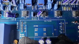
On the driver board there is this arrangement of zeners. It seems to trace out as I have drawn. Do these regulate the gate voltage? It seems that the lo side is within a volt at idle and that identical set of zeners seem to be taking the rail and dropping it down?
The hi side has the 11v dc offset between gate and source at idle.
On the driver board there is this arrangement of zeners. It seems to trace out as I have drawn. Do these regulate the gate voltage? It seems that the lo side is within a volt at idle and that identical set of zeners seem to be taking the rail and dropping it down?
Attachments
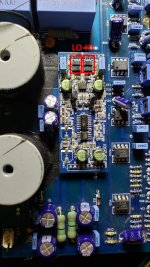

The zeners are a type of limiter. As long as they are not shorted, they aren't an issue.
Try connecting a 10k resistor between terminals 1 and 2 of the TL072 on the driver board.
Does that give you a drive signal?
Try connecting a 10k resistor between terminals 1 and 2 of the TL072 on the driver board.
Does that give you a drive signal?
- Home
- General Interest
- Car Audio
- Memphis PR1-1000 Zener ZD1 value?