The upper one is a 10M90 a 900v device,so that one can take the voltage.
the lower is 400v maybe it can take the voltage then,if not maybe I can use 10M90 as teh lower one to.
But I have it built with DN2540 as the lower one so it would be good if it could work wut that one.
the lower is 400v maybe it can take the voltage then,if not maybe I can use 10M90 as teh lower one to.
But I have it built with DN2540 as the lower one so it would be good if it could work wut that one.
The upper device in a cascode takes virtually all the voltage. I used DN2540 as lower device in a CCS with a 1100V B+ and I used a 1700V part above it. Worked fine, no issues.
The lower FET operating D-S voltage only few Volts.
The usual problem (not exactly in the linear range) is the low DS voltage (1.5-2V), not the overvoltage.
The usual problem (not exactly in the linear range) is the low DS voltage (1.5-2V), not the overvoltage.
Hi John,
When searching ISYS.COM for 1N100D2 I got “No matching parts, please modify your search criteria and try again.”
Is you sure this the right partnumber?
Regards, Gerrit
When searching ISYS.COM for 1N100D2 I got “No matching parts, please modify your search criteria and try again.”
Is you sure this the right partnumber?
Regards, Gerrit
You realize those symbols are enhancement mode? A depletion mode device has a continuous line for the channel to show it conducts at Vgs=0
When searching ISYS.COM for 1N100D2 I got “No matching parts, please modify your search criteria and try again.”
IXTP1N100D
So this IXTP1N100D N-channel MOSFET can be used instead of a 10M90S current source using the same schematic diagram? I’ve seen MOSFET’s exploding and would like to prevent this.
Regards, Gerrit
Regards, Gerrit
You realize those symbols are enhancement mode? A depletion mode device has a continuous line for the channel to show it conducts at Vgs=0
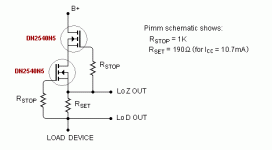
Please explain.The 10M90S is in top.
I have tried it on a PSU giving 65v and it seems to work.
How can I calculate how much of the voltage the upper device takes?
In your drawing, there is 2V across Rset. One hopes that an insignificant amount of current flows through both Rstops, so the gate of the upper fet is only 2V above the output of the CCS (for the 10.7mA case, for higher currents it won't even be 2V).
The source of the upper fet will be a couple of volts above its gate because it is running the same current and should have about the same Vgs, so now you're at a 4V difference compared to the output of the CCS. That's the boundary for the lower device. The rest gets dealt with by the upper device.
The bottom transistor sees just the gate to source voltage of the top one, so maybe 3V to 5V is dropped across it in order to turn on the top one. Lower one does not have to be high voltage at all.
You realize those symbols are enhancement mode? A depletion mode device has a continuous line for the channel to show it conducts at Vgs=0
Wow! I've been doing this almost 40 years and never knew that!
Pete
can the lower one be a jfet since it only takes several volts?
Yes. It can even be a device like an LM334. I've used the DN2540/LM334 cascode as an 1mA temperature compensated CCS to set a voltage across a resistor as a reference for a high voltage shunt regulator.
Okay thanks, That's good news. i have limited Dn2540 only 10 and 10M90s but have plenty of Jfets both high IDSS and Low IDSS types to combine with. Which is better the hi idss (like 2n4391 etc) or the lower IDSS Like 2sk30a ,2sk117)?Yes. It can even be a device like an LM334. I've used the DN2540/LM334 cascode as an 1mA temperature compensated CCS to set a voltage across a resistor as a reference for a high voltage shunt regulator.
On Current sinks i use Hi Idss but in this one I still have to experience..
- Home
- Amplifiers
- Tubes / Valves
- CCS maxvoltage?