Hello! This is my first post here. Nice to meet you.
This is a learn by doing project, a chance to learn how to use KiCad and also more about class AB amplifiers. Specifically the Boston Acoustics VR2000 subwoofer I have that needs repairs.
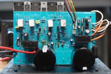
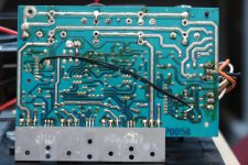
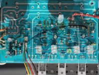
The images below are of the topside and underside of the circuit board, and I overlaid them on top of eachother in the third image to make following parts and traces easier. I drew a KiCad schematic with all the parts as best I could (keep in mind I'm new to the program!). The pdf of the schematic is attached. Some of the parts are difficult to read, especially the 5 color code resistors at times, so some of the values might not be correct. Also the output transistors are in pairs and I didn't feel like drawing extra stuff to keep it simple, so I labeled them and moved on.
Here are the problems. First, the bulk capacitors in the power supply were no good so I replaced C2 and C3. Then it worked for about a week or two, and broke again. The -12vdc voltage regulator failed, so I replaced both U2 and U3, along with their capacitors C13, C17, C18, and C19. Then it worked for a little while and broke again. Or maybe it broke again right away, I don't remember, I've been slowly working on this for a long time.
So right now the main power transistors on the negative rail (Q7/Q9) are shorted out and they pull enough current to blow the fuse moments after turning it on. The output transistors and the resistors on their base and emitter sides are all parallel. I didn't draw it perfectly since I'm barely hanging on to how this thing works, so I drew "Q7/Q9" and "R32/R33" instead of actually drawing out another set of parts.
I bought new transistors for both the + and - rails, a modern complimentary pair was recommended to me (2SC5200-OQ-ND and 2SA1943-OQ-ND). I'm ready to solder those in and see what happens, but that's $13 that can go up in smoke if I didn't fix the root cause, which I'm unsure of 😕
J26 goes to the DSP circuit board full of op-amps and other stuff I don't think is broken. U1 is a speaker protection chip that enables relay RL1 if everything looks good. Q3 and Q2 are part of some kind of feedback loop, I think. Q10 is for biasing the output transistors, I think. How can I tell if this potentiometer is set correctly? I've tried reading about setting bias currents, but I'm not sure how to apply that to this schematic. The bias adjustment is not on the output transistors, so where should I be measuring currents and such?
Yesterday I removed the final four power transistors and powered it up and it doesn't blow a fuse. I tried tracing the audio signal with an oscilloscope and I see a nice sine wave at "AudioToAmp" entering Q1 and Q2, then mostly square waves downstream of that. I'm not sure that's right. What should I see on a scope within the output transistor chain? I think it might change depending on if there is a load attached or not, is this right?
Last, near the power supply is some kind of voltage divider that is used by the feedback loop, formed by a resistor/zener pair Z1/R4 and Z2/R1. All four of those are discolored like they overheat often (see picture below). They may not be working as intended. I think those are zener diodes, but I could be wrong. What are those for, and how can I tell if they are working as intended?
Last last, all of the resistors are 5 band colors, and it's really hard to figure out what's what on some of them. I might have some values wrong somewhere.
Any other obvious things to look for before I solder the new power transistors back in?
Thank you all for the help 🙂
This is a learn by doing project, a chance to learn how to use KiCad and also more about class AB amplifiers. Specifically the Boston Acoustics VR2000 subwoofer I have that needs repairs.
The images below are of the topside and underside of the circuit board, and I overlaid them on top of eachother in the third image to make following parts and traces easier. I drew a KiCad schematic with all the parts as best I could (keep in mind I'm new to the program!). The pdf of the schematic is attached. Some of the parts are difficult to read, especially the 5 color code resistors at times, so some of the values might not be correct. Also the output transistors are in pairs and I didn't feel like drawing extra stuff to keep it simple, so I labeled them and moved on.
Here are the problems. First, the bulk capacitors in the power supply were no good so I replaced C2 and C3. Then it worked for about a week or two, and broke again. The -12vdc voltage regulator failed, so I replaced both U2 and U3, along with their capacitors C13, C17, C18, and C19. Then it worked for a little while and broke again. Or maybe it broke again right away, I don't remember, I've been slowly working on this for a long time.
So right now the main power transistors on the negative rail (Q7/Q9) are shorted out and they pull enough current to blow the fuse moments after turning it on. The output transistors and the resistors on their base and emitter sides are all parallel. I didn't draw it perfectly since I'm barely hanging on to how this thing works, so I drew "Q7/Q9" and "R32/R33" instead of actually drawing out another set of parts.
I bought new transistors for both the + and - rails, a modern complimentary pair was recommended to me (2SC5200-OQ-ND and 2SA1943-OQ-ND). I'm ready to solder those in and see what happens, but that's $13 that can go up in smoke if I didn't fix the root cause, which I'm unsure of 😕
J26 goes to the DSP circuit board full of op-amps and other stuff I don't think is broken. U1 is a speaker protection chip that enables relay RL1 if everything looks good. Q3 and Q2 are part of some kind of feedback loop, I think. Q10 is for biasing the output transistors, I think. How can I tell if this potentiometer is set correctly? I've tried reading about setting bias currents, but I'm not sure how to apply that to this schematic. The bias adjustment is not on the output transistors, so where should I be measuring currents and such?
Yesterday I removed the final four power transistors and powered it up and it doesn't blow a fuse. I tried tracing the audio signal with an oscilloscope and I see a nice sine wave at "AudioToAmp" entering Q1 and Q2, then mostly square waves downstream of that. I'm not sure that's right. What should I see on a scope within the output transistor chain? I think it might change depending on if there is a load attached or not, is this right?
Last, near the power supply is some kind of voltage divider that is used by the feedback loop, formed by a resistor/zener pair Z1/R4 and Z2/R1. All four of those are discolored like they overheat often (see picture below). They may not be working as intended. I think those are zener diodes, but I could be wrong. What are those for, and how can I tell if they are working as intended?
Last last, all of the resistors are 5 band colors, and it's really hard to figure out what's what on some of them. I might have some values wrong somewhere.
Any other obvious things to look for before I solder the new power transistors back in?
Thank you all for the help 🙂
Attachments
Last edited:
Square is normal due to feedback is cut without output transistors and it gives high gain. If you wanna try it that way you should bridge base to emitter pins (1-3) for both outputs AND disconnect the load, speakers or dummy load from output terminals.
!!! BUT BEFORE THAT !!! you should at first set the trimmer R29 in position of HIGHEST resistance, max. turn to that direction. Don`t miss that or you will have to buy new driver transistors. That setup should give you distorted sin wave output if you have sin at input. Maybe a fraction of oscillations too.
Than you can mount output transistors and set the bias current. So remove bridges and solder transistors.
Slowly turn the trimmer potty and measure voltage at R30/31 or R26/28.
12mV or 0.012V will give you 50mA bias current and is considered kind of standard. I would not go under 8mV or over 16mV for class AB.
Good luck
Thank you for the reply! This is wonderful.
That makes a lot of sense. I want to give that a try, but I'm also unsure about the voltage dividers formed by the resistor/diode pair at R1/Z2, and the matching pair on the negative rail. They are pretty discolored. How can I tell if they are working as they should be?
That makes a lot of sense. I want to give that a try, but I'm also unsure about the voltage dividers formed by the resistor/diode pair at R1/Z2, and the matching pair on the negative rail. They are pretty discolored. How can I tell if they are working as they should be?
Hello Justin, I'm not very experienced, but I noticed you have difficulty to red resistors sometime. Here is the solution (in this thread off topic) online: Resistor Color Code Calculator and Chart (4-band, 5-band or 6-band) - Electrical Engineering & Electronics Tools
When I mess up all my resistors, I check them three. Calculator woks well!
When I mess up all my resistors, I check them three. Calculator woks well!
When does this moderator-has-to-approve-every-post thing wear off? I can't find it in the faq or the forum rules.
I have read here that post approval status lasts a week before being eased. I imagine that's still discretionary though, depending on number of posts and what moderators consider acceptable behaviour etc.
I wouldn't doubt Digikey's quality system, its been spot-on spec, as has Mouser's over many years. Counterfeits are potentially everywhere else if you don't buy through major authorized distributors though. I don't worry too much over small signal parts which can easily be tested but power semi quality is expensive, critical and hard to prove without destructive tests. Buy safe or don't buy them at all if don't want to waste your money.
I wouldn't doubt Digikey's quality system, its been spot-on spec, as has Mouser's over many years. Counterfeits are potentially everywhere else if you don't buy through major authorized distributors though. I don't worry too much over small signal parts which can easily be tested but power semi quality is expensive, critical and hard to prove without destructive tests. Buy safe or don't buy them at all if don't want to waste your money.
Here is a tip I recently picked up .......... with the 4 output transistors removed temporarily solder a 1.5K resistor across the base and emitter solder holes of 2 of the output transistors , one across an NPN and another across a PNP . These resistors will simulate the base emitter junctions of the output transistors and complete the feedback loop and allow meaning full voltage measurements to be taken . Then carefully measure the DC voltages at the base , emitter and collector (with respect to ground) of all transistors including the simulated outputs . DC voltage readings are your friend in this situation .
Last edited:
MilanAudio, Thank you for the link but the challenge I have is determining which direction to read the colors. Some resistors have the two outside color bands the same width and symmetrically spaced so it is hard to tell which end is which.
Ian, thank you for the reply. I assumed Digikey would be a legitimate source for these parts and it seems it is.
I'll try overall feedback's idea soon and see how it goes.
I'm still curious about the R1/Z2 pair.
Ian, thank you for the reply. I assumed Digikey would be a legitimate source for these parts and it seems it is.
I'll try overall feedback's idea soon and see how it goes.
I'm still curious about the R1/Z2 pair.
I'm still curious about the R1/Z2 pair.
They are just a way of biasing this complementary input stage with push pull VAS, ref.. Bob Cordells Designing Audio Power Amplifiers book page 136.
Last edited:
> I'm still curious about the R1/Z2 pair.
If R1 and its twin are discolored, just replace them. 6K or so seems a fine value (not critical). They dissipate 1/3rd watt (maybe) so a 1/4W part is too small and a 1/2W part will not live forever; _I_ would go 1W here. (The equivalent circuit in many Fenders is known to crap-out after many years of hot living.) The obvious intent is to supply +/- stabilized voltages. My guess is they should be 15V each side, but Zener part-markings would be definitive. This should give a steady 15V each side (14V or 16V is all fine if steady).
If R1 and its twin are discolored, just replace them. 6K or so seems a fine value (not critical). They dissipate 1/3rd watt (maybe) so a 1/4W part is too small and a 1/2W part will not live forever; _I_ would go 1W here. (The equivalent circuit in many Fenders is known to crap-out after many years of hot living.) The obvious intent is to supply +/- stabilized voltages. My guess is they should be 15V each side, but Zener part-markings would be definitive. This should give a steady 15V each side (14V or 16V is all fine if steady).
I replaced the two resistors in the R/Z pairings and the voltage measures 20v and 24v on each. A bit more than 15v, and not really matching eachother. I hope this is reasonable.
I also shunted the base/collector on the output transistor pads on the board with a 1k resistor and increased the bias potentiometer to maximum resistance. The amplifier now passes a nice looking sine wave through to the output. Fantastic, thank you all for the help.
I ran out of time to play today, so I will put the new transistors on the board and redo the heatsink grease, then adjust the bias to about 50mA as seems common.
I also shunted the base/collector on the output transistor pads on the board with a 1k resistor
Is this a typo I suggested base/emitter .
I also shunted the base/collector on the output transistor pads on the board with a 1k resistor and increased the bias potentiometer to maximum resistance. The amplifier now passes a nice looking sine wave through to the output.
Have you checked the DC offset on the output with the base/emitter resistors in place.
Last edited:
I have not. What sort of DC offset should I expect to see? I assume this is with either no signal or a small signal being passed through?
Some where in the 10s of millivolts region the lower the better . What I want to make sure is that you don't have a significant DC offset in the whole Volts region before you put your new output trannies in . Check with no signal on the input and/or short circuit the input .
Last edited:
I put the bypass resistors back on the circuit board between the output transistor pads base/emitter pins 1+3. I shorted the audio inputs to input ground and the trace labeled as "AudioToAmp" is very quiet. The bias adjustment potentiometer is set at maximum resistance between Q10 pins 1+3. I have also replaced R4 and R1.
The attached PDF shows DC voltages measured at each pin of each transistor on the drawing, and a couple other spots too.
The attached PDF shows DC voltages measured at each pin of each transistor on the drawing, and a couple other spots too.
Attachments
- Home
- Amplifiers
- Solid State
- I reverse engineered the schematic, now I need some help with troubleshooting AB amp