Hey guys,
I've gone and applied 12V to my 5V input. Opened her up and saw this "rectifier" looking component has popped. I can't tell the markings and it's different from the other one beside it. Any ideas? I've looked for some pics on this forum but can't find a good pic of this component. It's right here at the DC input.
Would love to repair this.
Hi mrgarison,
Maybe someone can post a picture of a healthy E30. You should email Topping a picture and description of what happened. They won't release schematics last time I checked. If they are half-way responsible they might tell you what that part is.
Maybe someone can post a picture of a healthy E30. You should email Topping a picture and description of what happened. They won't release schematics last time I checked. If they are half-way responsible they might tell you what that part is.

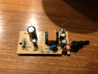
A1 noted on top crosses to a dual general purpose switching diode, BAW56 in the SOT23 package. A typical BAW56 device has a rating of 215mA with a surge of 4A. That makes sense in the location it is used near the power input and capacitors.
It may be like this one at Mouser: https://www.mouser.com/ProductDetail/Nexperia/BAW56235
Hopefully you can get a confirmation in an email from Topping.
It may be like this one at Mouser: https://www.mouser.com/ProductDetail/Nexperia/BAW56235
Hopefully you can get a confirmation in an email from Topping.
The A1 is more likely a transistor.
It could be an Si2301DS, a P-channel MOSFET, -20V and around 2A.
The pin on the top-left would then be the source. And there seems to be a 10k resistor (01C) between the source and the gate, to turn it off, unless turned on by being pulled low by the "Y1" transistor (most likely an NPN transistor controlled via the 1k resistor (01B).
The question is of course also: why did it fail? Did something after the power switch fail (short circuit) first?
Is there a zener diode or similar to prevent overvoltage? And if so, did that that zener diode survive?
The question is of course also: why did it fail?
...I've gone and applied 12V to my 5V input.
//
That alone should not cause such damage if the MOSFET max VDS is -20V. Quite likely something else was zapped as well.
Yes, I saw that 12V had been applied.
But 12V is in-itself not enough to destroy a 20V FET. A high current must have been flowing in the FET. And did that destroy something further down the line, so that a new FET will be destroyed immediately, even with 5V applied? Or did the parts after the FET power switch survive?
But 12V is in-itself not enough to destroy a 20V FET. A high current must have been flowing in the FET. And did that destroy something further down the line, so that a new FET will be destroyed immediately, even with 5V applied? Or did the parts after the FET power switch survive?
You pooped the bed.
We need a picture of a good one. I think it is a Richtek brand regulator.
We need a picture of a good one. I think it is a Richtek brand regulator.
Give it some time. Someone may be able to measure it for you.
Best to work from a position of knowledge than guesses.
Best to work from a position of knowledge than guesses.
The topology clearly shows a load switch, with a P-channel FET and an NPN transistor to turn it ON/OFF.
The PNP transistor is most likely controlled by the STM microcontroller.
See the figure below.

Replacing the FET should not be too difficult, but I am worried that several other components may have been damaged.
There are a number of voltage regulators that may have been damaged. So far I have not been able to identify the part types.
The supply for the micro controller looks like an LDO, marked AD.
The supply for the XMOS seems to be a dual step down converter, marked AEDJ (I think).
And then there is an IC marked DP0 3S8, which most likely generates the +/- supplies for the analog parts (op-amps). +5.65V, -5.6V for op-amps and +10V for the SGM3710.
There is also a 3.3V LDO, marked S35G. If that is also supplied from the switched DCIN (which was subjected to 12V), it may also have been destroyed, unless it is a wide-vin type.
If the switch mode converters and LDO's can be identified, it will be easier to guesstimate if they survived the 12V.
Worst case the 12V also got past the regulators. Then it becomes difficult.

The PNP transistor is most likely controlled by the STM microcontroller.
See the figure below.
Replacing the FET should not be too difficult, but I am worried that several other components may have been damaged.
There are a number of voltage regulators that may have been damaged. So far I have not been able to identify the part types.
The supply for the micro controller looks like an LDO, marked AD.
The supply for the XMOS seems to be a dual step down converter, marked AEDJ (I think).
And then there is an IC marked DP0 3S8, which most likely generates the +/- supplies for the analog parts (op-amps). +5.65V, -5.6V for op-amps and +10V for the SGM3710.
There is also a 3.3V LDO, marked S35G. If that is also supplied from the switched DCIN (which was subjected to 12V), it may also have been destroyed, unless it is a wide-vin type.
If the switch mode converters and LDO's can be identified, it will be easier to guesstimate if they survived the 12V.
Worst case the 12V also got past the regulators. Then it becomes difficult.
A new Topping E30 Mk II costs 149 Euro. This one may be repairable but at what cost and how are the chances it will be 100% OK? I had an SMSL DAC that was zapped and even AK4493 was kaput.
Removing the defective part and shorting its source to drain will tell.
BTW one starts to like internal PSUs after incidents like this.
Removing the defective part and shorting its source to drain will tell.
BTW one starts to like internal PSUs after incidents like this.
Last edited:
I just should have looked. I was let down by the dang barrel connector. I just assume any of those are 12 V. From the day I got this I was perplexed why they would choose to use a barrel connector rather than USB C or a heftier USB-B.
Yeah nobody uses these 😉
Assumptions and mixing up of adapters/SMPS are a bit fatal. It helps to have a label on the cable with the device name.
Sometimes they are so light you just know something is not right. This one is new but look what was omitted. The right habit is then to pick one based on voltage and current. Only current may be higher. Higher voltage is bad. Only then check the barrel connectors size (and polarity!) and choose a better quality one. Not to pick a random 12V or 24V one with a barrel connector that fits OK.
Also plugging in random connectors in random devices out of pure lust or promiscuity may lead to the feared connector-AIDS. Most couples are quite monogamous. One better not separates them so they’ll have a long happy lifetime.
Attachments

Last edited:
https://www.aliexpress.com/item/100...7*MTczMjE2OTAxMi4yLjEuMTczMjE2OTQ3Ny41Ny4wLjA.The topology clearly shows a load switch, with a P-channel FET and an NPN transistor to turn it ON/OFF.
The PNP transistor is most likely controlled by the STM microcontroller.
See the figure below.
View attachment 1382984
Replacing the FET should not be too difficult, but I am worried that several other components may have been damaged.
There are a number of voltage regulators that may have been damaged. So far I have not been able to identify the part types.
The supply for the micro controller looks like an LDO, marked AD.
The supply for the XMOS seems to be a dual step down converter, marked AEDJ (I think).
And then there is an IC marked DP0 3S8, which most likely generates the +/- supplies for the analog parts (op-amps). +5.65V, -5.6V for op-amps and +10V for the SGM3710.
There is also a 3.3V LDO, marked S35G. If that is also supplied from the switched DCIN (which was subjected to 12V), it may also have been destroyed, unless it is a wide-vin type.
If the switch mode converters and LDO's can be identified, it will be easier to guesstimate if they survived the 12V.
Worst case the 12V also got past the regulators. Then it becomes difficult.
View attachment 1382985
I think I found it thanks to your photo. I appreciate the help! Ordered it, should arrive in a couple weeks. Fingers crossed it didn't blow anything else.
Just assume it is beyond repair and that you learn from the experience. The only times I only need to replace one part is when the devices are not mine 😀
- Home
- Source & Line
- Digital Source
- Topping E30 Pooped The Bed