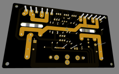
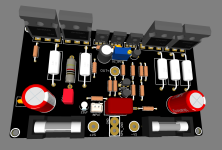
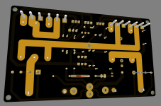
One thing I see- You generally want to use a "star ground" that centers on the negative side of the power bypass capacitor(s), so that the drivers and pre-drivers each have an independent path to ground, so the power drivers are not inducing an AC IR drop in their ground path that will bounce the ground of the pre-drivers. The grounds for the input, the diff pair (R1=22k, C3=22uf) and for bias R7=2.2K should not go to the GND/SPK_GND point which will be bouncing, but to the ground side of the two bypass caps which will be actual AC ground. There will be a large AC current between the GND/SPK_GND and the negative side of the bypass caps, so to minimize AC IR drop, this ground trace should be the same wide width as for the supply trace.
That's about all I can see. Great work!
That's about all I can see. Great work!
You'd get better performance with a ground plane than with a star ground. Just make sure that quiet grounds are in an area of the ground plane where you have low current density. Alternatively pour a quiet ground on the bottom of the board and a ground plane on the top of the board for the dirty ground. Anything input-referenced connects to the quiet ground. Everything else, including the feedback ground, connects to the dirty ground.
Having V+ and V- on opposite ends of the board will result in the highest rail-induced distortion. you really want to run V+ and V- stacked or side-by-side. Douglas Self writes quite a bit about that in his power amps book (and Wireless World articles that led to the book).
I'd also get rid of the slot for C3. Either pick a capacitor and use a matching footprint or have a string of holes on 0.1" grid.
Tom
Don't know the amp in question so just some mechanical thoughts:
- do you have enough room around your mounting holes to put a washer under your screws and will the bottom traces not be touched by mounting pillars?
- having your transistors not at the edge will make it harder to mount them on a heatsink. And the BD's are not on the same line as the TIP's. A 2-layer pcb is hardly more expensive and much more stable.
Good catch about the traces close to the mounting holes. It also looks like those holes are very close to the board edge. I generally use 3.2 mm diameter holes centred 5 mm from the board edges.
You're using a spade for the speaker ground but a single hole for the speaker output. It looks like you have room for a spade at the output.
Are you sure you have enough room for the 5 W resistors? They should have some breathing room. I usually also add a vent hole below the resistors to promote the chimney effect.
I recently priced 1-layer and 2-layer boards at a few overseas outfits. All of them charged the same for a 1-layer board as they do for a 2-layer board. So if you're having the boards manufactured professionally you might as well use both layers. You pay for the copper either way. The only difference is how much of it is dissolved in the acid during etching. Two-layer boards aren't hard to make even if you etch them yourself.
Tom
Tom you know as well as I that making your own pcbs, esp two layers is a real pita. That and buying from jlcpcb or others is actually cheaper than the cost of the materials to make your own.
One thing I see- You generally want to use a "star ground" that centers on the negative side of the power bypass capacitor(s), so that the drivers and pre-drivers each have an independent path to ground, so the power drivers are not inducing an AC IR drop in their ground path that will bounce the ground of the pre-drivers. The grounds for the input, the diff pair (R1=22k, C3=22uf) and for bias R7=2.2K should not go to the GND/SPK_GND point which will be bouncing, but to the ground side of the two bypass caps which will be actual AC ground. There will be a large AC current between the GND/SPK_GND and the negative side of the bypass caps, so to minimize AC IR drop, this ground trace should be the same wide width as for the supply trace.
That's about all I can see. Great work!
You'd get better performance with a ground plane than with a star ground. Just make sure that quiet grounds are in an area of the ground plane where you have low current density. Alternatively pour a quiet ground on the bottom of the board and a ground plane on the top of the board for the dirty ground. Anything input-referenced connects to the quiet ground. Everything else, including the feedback ground, connects to the dirty ground.
Having V+ and V- on opposite ends of the board will result in the highest rail-induced distortion. you really want to run V+ and V- stacked or side-by-side. Douglas Self writes quite a bit about that in his power amps book (and Wireless World articles that led to the book).
I'd also get rid of the slot for C3. Either pick a capacitor and use a matching footprint or have a string of holes on 0.1" grid.
Tom
Don't know the amp in question so just some mechanical thoughts:
- do you have enough room around your mounting holes to put a washer under your screws and will the bottom traces not be touched by mounting pillars?
- having your transistors not at the edge will make it harder to mount them on a heatsink. And the BD's are not on the same line as the TIP's. A 2-layer pcb is hardly more expensive and much more stable.
Good catch about the traces close to the mounting holes. It also looks like those holes are very close to the board edge. I generally use 3.2 mm diameter holes centred 5 mm from the board edges.
You're using a spade for the speaker ground but a single hole for the speaker output. It looks like you have room for a spade at the output.
Are you sure you have enough room for the 5 W resistors? They should have some breathing room. I usually also add a vent hole below the resistors to promote the chimney effect.
I recently priced 1-layer and 2-layer boards at a few overseas outfits. All of them charged the same for a 1-layer board as they do for a 2-layer board. So if you're having the boards manufactured professionally you might as well use both layers. You pay for the copper either way. The only difference is how much of it is dissolved in the acid during etching. Two-layer boards aren't hard to make even if you etch them yourself.
Tom

I actually don't find it that hard. I've been making 2-layer boards in my garage (or kitchen!) fab for 20+ years. With toner transfer I was able to get ±0.1-0.2 mm registration between the top and bottom layer. I just attached the layouts to a scrap piece of circuit board and made sure they were aligned before feeding the board through the laminator.Tom you know as well as I that making your own pcbs, esp two layers is a real pita.
I did keep the possibility of garage fab in mind when I wrote above. You can easily make a ground plane by leaving the copper un-etched on one layer. Etch the other layer and drill the holes. Then use a larger drill bit to create little "countersinks" where you don't want the copper to connect to component pins. Solder on both layers.
Etching one layer is easy. Just let the board float on the etchant.
I don't think I've ever had to pay for the raw PCB material. I dumpster dove a bunch of scraps in college and have several sheets that I bought at a surplus auction at TI. Hydrochloric acid and hydrogen peroxide are pretty cheap. If I had to source PCB materials too, I would have stopped making my own boards sooner.That and buying from jlcpcb or others is actually cheaper than the cost of the materials to make your own.
That said, the garage fab is pretty messy and the results are usually okay-ish at best. I haven't etched my own board in nearly ten years now. Having 'real' boards with solder mask, gold plating, etc. is just so much nicer to work with. I spend less time sorting out board issues, which means I can spend more time designing and debugging circuits. Even with fast shipping the cost of boards from the overseas places are dirt cheap and the quality is certainly good enough for prototypes.
I have had a couple of issues with the cheap overseas outfits, which is one of the reasons the boards I sell have been made in Canada for 6-7 years now. I also pay extra to have the boards electrically tested, which adds cost up front but saves money in the long run as I know the boards are good before I send them off to assembly.
Tom
hi to everyone guys, Ciro, if I may: as someone has already suggested to you: I would suggest you to create two diffuse ground plane layers (top and bottom) connected to each other with multiple vias throughout the PCB. In addition to electrical advantages (lower return impedance of signals, protection against electromagnetic interference) you will certainly have more space available to optimize placecement of components and tracks. It's just a suggestion of course . Nice day
Ros
Ros
Ok Ciro82- In the latest layout- looking better. The three smaller ground traces that meet the big ground trace in the lower left corner- They should go right to the negative side of the bypass capacitor directly, not the middle of the ground trace between the ground terminal and the bypass cap. The negative side of the bypass cap will be the quietest place. As large pulses of current are driven through out, through the speakers, and back into the ground terminal, there will be large pulses of current between the negative side of the bypass and that ground terminal as the capacitor sloshes charge back and forth through the trace trying to hold the voltage constant. That part of the trace will have some (small) IR drop between the ground terminal and the negative side of the cap. The typical star ground converges right on the negative side of the bypass, and all ground traces independently meet there. You have a second bypass cap on the right, which also has a negative side, and that can be used as well.
The idea of a ground plane can be useful, but it really depends upon how dense the routing on the board is. I have seen ground planes become swiss cheese because they are so broken up. If you have a relatively low density side that might be a good place. Make sure the fundamentals are correct, (star ground, avoiding IR drops and inductive loops, coupling if high frequency) and a ground plane is not necessary. For this application we are pretty much just polishing the brass tacks as far as IR drops. As long as all of the other concerns are addressed (component size and breathing, room around screw locations, etc,) I think you are pretty close.
The idea of a ground plane can be useful, but it really depends upon how dense the routing on the board is. I have seen ground planes become swiss cheese because they are so broken up. If you have a relatively low density side that might be a good place. Make sure the fundamentals are correct, (star ground, avoiding IR drops and inductive loops, coupling if high frequency) and a ground plane is not necessary. For this application we are pretty much just polishing the brass tacks as far as IR drops. As long as all of the other concerns are addressed (component size and breathing, room around screw locations, etc,) I think you are pretty close.
I agree. Also, especially with PTH components, the component orientation can mean the difference between a ground plane that's decent and one that's useless.The idea of a ground plane can be useful, but it really depends upon how dense the routing on the board is. I have seen ground planes become swiss cheese because they are so broken up.
But in this case, the layout is currently single-layer, so the potential for a solid ground plane exists. That would be a few orders of magnitude better than the current star ground.
The current layout is still the worst case for rail-induced distortion. Also, the current that will flow in the ground from the 220 uF decoupling caps can be pretty gnarly. That will corrupt the star ground. It would be better to place the two 220 uF (and two 100 nF) side-by-side and run the power up the middle of the board. Or run the power from one side of the board.
I would also like to get the power devices closer to the edge of the board. You'll have to stretch and possibly extend the pins of the BD139s to make them reach the heat sink. That's not ideal.
Tom
- Home
- Amplifiers
- Solid State
- PCB layout advices - Rod Elliott P10

