Greetings and Salutations,
I am interested in understanding the continuous DC SOA of the KSC2690A transistor. I am unable to figure out what I am allowed to push at what voltage without looking at the maximum allowed TPD.
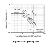
The SOA graph includes a curve for DC, but it’s labeled as "dissipation limited," which makes sense; however, it also includes "PW = 50 ms" on the same line, which isn’t DC. Additionally, it’s marked "S/b limited," which I haven't encountered before—I assume it might mean silicon/bond wire limitation?
Am I allowed to operate at 0.1A @ 100V Vce? This would result in a dissipation of 10W, while the datasheet allows a maximum dissipation of 20W if the case is maintained at 25°C.
Thank you in advance, and best regards from Germany!
I am interested in understanding the continuous DC SOA of the KSC2690A transistor. I am unable to figure out what I am allowed to push at what voltage without looking at the maximum allowed TPD.
The SOA graph includes a curve for DC, but it’s labeled as "dissipation limited," which makes sense; however, it also includes "PW = 50 ms" on the same line, which isn’t DC. Additionally, it’s marked "S/b limited," which I haven't encountered before—I assume it might mean silicon/bond wire limitation?
Am I allowed to operate at 0.1A @ 100V Vce? This would result in a dissipation of 10W, while the datasheet allows a maximum dissipation of 20W if the case is maintained at 25°C.
Thank you in advance, and best regards from Germany!
Attachments
S/b must be second breakdown. It's a set of current crowding effects that much reduce the current bipolar transistors can handle at high collector-emitter voltages.
In the case of thermal second breakdown, when a small area on the transistor draws a bit more current than the rest, it will get a bit hotter than the rest. The higher temperature will increase the current through that area, which will increase the temperature again. It's essentially positive feedback; if the loop gain is greater than one, the temperature of the hot spot keeps increasing until the transistor is destroyed.
MOSFETs used not to have this issue, but that is no longer true since the mid-1990's. The efforts of the manufacturers to reduce the on resistance of switching MOSFETs has made many types of switching MOSFETs with a really low on resistance very sensitive to thermal runaway. For some reason it is called Spirito instability instead of second breakdown for MOSFETs, after the person who discovered the issue.
Regarding that 50 ms, I guess it means that the manufacturer has done the DC destructive characterization testing with 50 ms pulses. Theoretically they should have used infinitely long pulses, but that is of course not practical. Apparently they have the experience that if a transistor blows up, it does so within 50 ms.

I'm not sure if and how much the second breakdown figures need to be derated for higher junction temperatures. I hope someone with more experience with bipolar power transistors can answer that.
If they don't need to be derated much, the transistor can handle 100 mA at 100 V with good cooling. You will have to ensure that the power (10 W) times the sum of the thermal resistances from junction to case, case to heatsink and heatsink to ambient is less than the difference between the maximum rated junction temperature and the maximum ambient temperature.
If they don't need to be derated much, the transistor can handle 100 mA at 100 V with good cooling. You will have to ensure that the power (10 W) times the sum of the thermal resistances from junction to case, case to heatsink and heatsink to ambient is less than the difference between the maximum rated junction temperature and the maximum ambient temperature.
Thank you!If they don't need to be derated much, the transistor can handle 100 mA at 100 V with good cooling. You will have to ensure that the power (10 W) times the sum of the thermal resistances from junction to case, case to heatsink and heatsink to ambient is less than the difference between the maximum rated junction temperature and the maximum ambient temperature.
I know that. This will only happen if another transistor shorts out in my circuit. I prefer to select transistors (when possible) in a way that, if something goes wrong for some reason, it won’t create a chain reaction and destroy all other components but will instead stop at a certain point.
You mean they are testing each transistor in the production line like that? I though they only test the transistors while prototyping and make these graphs. And only test the transistors for functionality in the production line?Regarding that 50 ms, I guess it means that the manufacturer has done the DC destructive characterization testing with 50 ms pulses. Theoretically they should have used infinitely long pulses, but that is of course not practical. Apparently they have the experience that if a transistor blows up, it does so within 50 ms.
As far as I know the destructive tests are only done on prototypes, but on quite a lot of prototype transistors. There are many combinations of voltage and current that need to be tested and they need to get a good idea of the variations between samples, so they can calculate what values they can guarantee and put in the graph.
NoAm I allowed to operate at 0.1A @ 100V Vce? This would result in a dissipation of 10W, while the datasheet allows a maximum dissipation of 20W if the case is maintained at 25°C.
Transistors don't stay at 25c
Specially with 100mA of current.
40c to 70c to be expected.
Data sheet has a derating curve. Generalized about 80 to 60% de rate
for 45 to 75c
looking at 25c chart at 100mA with 100 volts its darn well already close to instantly failing.
Already borderline at 25c
Its a 1.5 watt transistor as rated in the datasheet.
Or just a T0-126
As with most T0-126 in a amplifier wouldn't have DC bias much higher than 6mA to 10mA
and depending on the load your driving. Expect 18 to 20mA of AC current.
So dont expect more than 30/ 40 mA total from a T0-126 to be safe at temperature with high voltages.
At least for many famous high speed Fairchild transistors like this or 3503 or 1381
they are basically T0-92 type wafers mounted on a T0-126 case to be more robust.
Many of them were originally T0-92M package which is slightly bigger longer TO-92
20 watts is absolute max rating at 25c and a complete fantasy. We use average dissipation 1.5 watts at 25c and derate from there 60 to 70% at temp
The thermal time constant inside the package is pretty fast. In 50 ms, it heats up damn near to full temperature internally. Hence, the 50 ms curve is not that far above the continuous. “Audio signals” often use the 10ms curve for instantaneous dissipation and peak junction temp - as most of the signal peaks won’t be any longer than that. By “signal peak” we mean instantaneous I*V values.
The thermal derating curves are just linear approximations. It’s considered “good enough” in lieu of a full thermal model. Basically, derate linearly to zero at the max rated temp. The second breakdown limited portion of the curve generally derates differently - but the temperature rise usually overtakes this. As the old Motorola data sheets state “At high case temperatures, thermal limitations will reduce the power that can be handled to values less than the limitations imposed by second breakdown”. For devices or applications where this is NOT typically the case, they provide a second-breakdown derating curve. For audio use, one can generally use the 10 ms curve thermally limited portion of the curve and derate it for temperature. Where it intersects the second breakdown limited portion is the new breakpoint. Some DIY designers will start at the DC curve and derate from there to be conservative. No one in the commercial world does, unless the amp is intended to work down to DC or damn near it. Even a 20 Hz sine wave at half the available peak voltage doesn’t hold at the maximum dissipation very long.
Manufacturers do a lot of destructive (sometimes non destructive) testing to arrive at the curves for second breakdown. There is a way to test for it non destructively, but it’s only good in an engineering lab type environment. Some parts are 100% tested at single points, and it’s a go/no go. They don’t do it much anymore - the last ones to say so on the data sheets were MJ15024’s.
So it seems like I have to go with a to220 package to ensure that this transistor will hold up, if something dies and 100mA @ 100V pass through it.
Thank you all!
Thank you all!
Last edited:
It's on the edge. Maybe it will just do if you manage to keep the case temperature below 70 degrees Celsius during this fault condition.
According to this datasheet:
https://www.mouser.com/datasheet/2/149/KSC2690A-88885.pdf
the maximum power dissipation at 25 degrees Celsius case temperature is 20 W and the maximum junction temperature is 150 degrees Celsius. As usual and as shown in figure 7, the power has to be derated via a straight line segment to zero at a case temperature equal to the maximum junction temperature. That means it can handle 10 W up to 87.5 degrees Celsius case temperature.
The SOAR graph in figure 6 shows it can handle about 0.13 A at 100 V, second breakdown limited. This must be at 25 degrees case temperature, because the power-dissipation-limited part of the DC SOAR curve corresponds to 20 W.
Figure 7 shows that second-breakdown current has to be derated to about 75 % at 87.5 degrees case temperature. 75 % of 130 mA is 97.5 mA, but the value on the SOAR curve might just as well be 120 mA (hard to see on a logarithmic scale), in which case 75 % is only 90 mA. In that case, you would need to keep the case temperature below about 70 degrees Celsius to get it at 100 mA.
Normally it would be a bad idea to load devices to the very limit because it affects reliability and lifetime, but that doesn't apply in this case, as you only load it that much during a fault condition.
Last edited:
- Home
- Design & Build
- Parts
- KSC2690A SOA - help needed to understand the datasheet