Hello everyone
I'm repairing a clone BASSFACE 3000W class D mono block with dead power supply and output section.
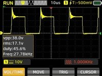
When I fitted the new FETs and drivers, I noticed big inductive spikes on the drains of the power supply mosfets.
I already brought down the frequency to 20 KHz to minimize the effect on the mosfets.
Is there any way to get rid of these spikes or it's just a bad design of the transformers and nothing could be down for it?

I'm repairing a clone BASSFACE 3000W class D mono block with dead power supply and output section.
When I fitted the new FETs and drivers, I noticed big inductive spikes on the drains of the power supply mosfets.
I already brought down the frequency to 20 KHz to minimize the effect on the mosfets.
Is there any way to get rid of these spikes or it's just a bad design of the transformers and nothing could be down for it?
Attachments
Last edited:
Ferrite beads around mosfet gates may help... difficult to predict the result... because all those gates are connected in parallel via long PCB copper traces, coming from the switching IC. You could try to dampen the ringing at the switching IC (27.8kHz oscillator) as well.... Try the beads first and see... (look at the oscilloscope for dampened rising edge ringing)

At 7V of input, it turns on fine and there are no voltage spikes at the top of the drain waveform. However, as soon as the voltage is increased to 12V, they appear, and the amplifier draws 12A of current!Ferrite beads around mosfet gates may help... difficult to predict the result... because all those gates are connected in parallel via long PCB copper traces, coming from the switching IC. You could try to dampen the ringing at the switching IC (27.8kHz oscillator) as well.... Try the beads first and see... (look at the oscilloscope for dampened rising edge ringing)
Any idea what this is all about?
Is my understanding correct that a bad transformer design is causing these parasitic inductances to form and oscillate at the top of the drains of the FETs?
This board doesn't have any snubber network...While replacing MOSFETs (especially with different ones), it may be necessary to redesign / adjust the snubbing as well.
I replaced them with the same part number
Output also had a step on the gates signal and needed more powerful drivers.
This isn't a very well designed board...
You might want to add one in order to avoid further failures.This board doesn't have any snubber network...
https://e2e.ti.com/cfs-file/__key/communityserver-discussions-components-files/196/RC-Snubber.pdf
If the step was on the turn-on transition of the gate, then that's Miller effect but my guess is that the turn-off resistor needs to increase a bit, especially if it's a push-pull converter.Output also had a step on the gates signal and needed more powerful drivers.
Changing the driver transistors to TO220 package type from TO92 actually solved the problem, my guess was that the driver transistors couldn't deliver enough current during the turn-on of the FETs.If the step was on the turn-on transition of the gate, then that's Miller effect but my guess is that the turn-off resistor needs to increase a bit, especially if it's a push-pull converter.
Thanks for the suggestion, I will definitely add a snubber network, hope this helps.You might want to add one in order to avoid further failures
Any other suggestions on how to improve on it?
I also changed the gate resistors from 10 to 100 Ohm to soft drive the FETs and changed the drivers from BC327 TO B772 and pull down transistors from 2N4401 to D882.
I just wanted to give an update on the situation.
With the help of the Sam at Barevids YouTube channel I found out that the spikes is mainly due to the high duty cycles and some other design issues that I solved and now it's operating at its optimum conditions and the voltage spikes are completely gone.
I reduced the duty cycle to 35-40% (depending on the input voltage) and changed the drive and pull down transistors with better ones and changed the gate resistors back to 10 Ohm.
- Home
- Amplifiers
- Class D
- Voltage spikes on power supply mosfets drains