The AD811 has a relatively high quiescent current (over about 15 mA) and heats to about 50-60°C. The IC can certainly withstand this temperature but I'm a bit concerned about the performance degradation associated with the temperature increase.

That's an interesting solution.
I never used thermal epoxy, that would be a challenge for me, which tools can be used? Is there any risk of damaging the IC during the procedure?
I never used thermal epoxy, that would be a challenge for me, which tools can be used? Is there any risk of damaging the IC during the procedure?
Two part thermal epoxy can be used like regular epoxy, and cured at room temp.
It just conducts heat better. You'd only need a couple of drops for one IC package, though.
It just conducts heat better. You'd only need a couple of drops for one IC package, though.
Is it better or worse than thermal paste in terms or thermal resistance?
What are the main advantages of thermal epoxy?
What are the main advantages of thermal epoxy?
Purpose of thermal epoxy is to conduct heat between the two surfaces that are glued together.
Much more so than regular epoxy.
Much more so than regular epoxy.
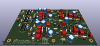
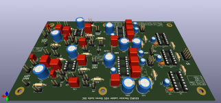
I've finished the draft of the schematic and PCB layout of my first prototype board based on the PCB design made by miro1360 for the AD1862.I think I can base my DAC board on the lastest version of miro1360, if he allows me to do so, but I want to simplify the logic section and modify the I/V stage to be able to accommodate a CF opamp, like the AD811.
The preamp board I will try to design myself from scratch.
Since I'm a noob I'm sure it must be full of design flaws. 😋
The PCB is also very large, since I've included a lot of jumpers to test both onboard (with several different opamps, VF and CF types) and external I/V stages.
For now I'm not thinking about including the PDIP heatsink for the I/V stage opamps.
Could you take a look and try to spot the mistakes and what can be improved?
I've used KiCad, which is not a very popular tool for PCB design, so I have attached some pictures of the schematic and the gerber files of the PCB layout draft.
I haven't had enough time to draw the preamp PCB yet.
Attachments
-
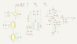 Logic Section and left channel.png63.5 KB · Views: 77
 -
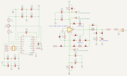 Right channel.png16.8 KB · Views: 65
 -
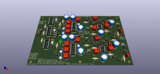
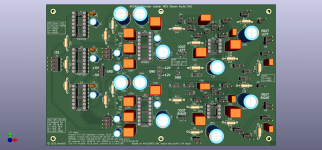 AD1862_v1_draft_3D_front.png179.3 KB · Views: 71
 -
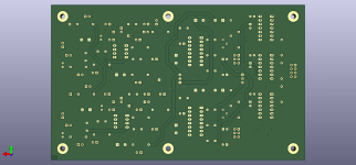
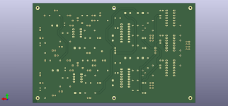 AD1862_v1_draft_3D_back.png95.8 KB · Views: 73
 -
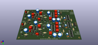
 AD1862_v1_draft_3D_front_perspective1.png147.9 KB · Views: 66
 -
 AD1862_v1_draft_3D_front_perspective2.png150.7 KB · Views: 65
 -
Gerbers.zip382.4 KB · Views: 57
Some generic comments regarding pcb:
Even if not ideal in terms of performance, your jumpers will allow you to assess and make your own opinion on the various options implemented in your schematic; that's a good point. Rather than using pin header you can use solder jumper which are smaller, cheaper, etc. Those are standards footprints available in Kicad, see pic:

I’ve recently read, that supply decoupling of the 5534 or 32 is preferably made with cap between V+ and V- rather than caps relative to ground. If you have some room, you can add a 100n between pins 4&7 of your opamp sockets.
Your fixing holes look small, are they at least 3- or 3.5-mm diameter? This is common value for fixing screws.
It looks like all (or most of) your ground connection are made with the ground plane. Ok but, unfortunately it is interrupted by vertical tracks. One AD1862 is stuck in a quasi ‘ground island’ (U4). Without redrawing the all pcb, the situation could be improved by adding ground ‘bridges’ to jump over the verticals tracks. Use vias to build those bridges. See pic for suggestions where to place bridges:

One other improvement, but more difficult to achieve, is to separate digital and analog ground. That’s start in the schematic where the two grounds should be identified separately and connected to the right parts: analog ones and digital ones, with the AD1862 which uses both. Then pcb should be redrawn and both grounds connected together in a single point. Miro implementation does not separate grounds, so…it should be alright, you may forget this !
Even if not ideal in terms of performance, your jumpers will allow you to assess and make your own opinion on the various options implemented in your schematic; that's a good point. Rather than using pin header you can use solder jumper which are smaller, cheaper, etc. Those are standards footprints available in Kicad, see pic:
I’ve recently read, that supply decoupling of the 5534 or 32 is preferably made with cap between V+ and V- rather than caps relative to ground. If you have some room, you can add a 100n between pins 4&7 of your opamp sockets.
Your fixing holes look small, are they at least 3- or 3.5-mm diameter? This is common value for fixing screws.
It looks like all (or most of) your ground connection are made with the ground plane. Ok but, unfortunately it is interrupted by vertical tracks. One AD1862 is stuck in a quasi ‘ground island’ (U4). Without redrawing the all pcb, the situation could be improved by adding ground ‘bridges’ to jump over the verticals tracks. Use vias to build those bridges. See pic for suggestions where to place bridges:
One other improvement, but more difficult to achieve, is to separate digital and analog ground. That’s start in the schematic where the two grounds should be identified separately and connected to the right parts: analog ones and digital ones, with the AD1862 which uses both. Then pcb should be redrawn and both grounds connected together in a single point. Miro implementation does not separate grounds, so…it should be alright, you may forget this !
Thank you very much for the tips AIM65, you've made a thorough analysis. 👍
I never used ground bridges, how are they made, is it just a matter of connecting the top and bottom ground planes using vias or is it more complex than that? Could you please, explain it better or give me an example?
Yes, well spoted, it was a compromise that I've made to increase the board's flexibility, since this version is meant to be a prototype for testing different I/V stages and possibly external digital signal sources. I'm not very familiar with solder jumpers, I think they must perform better, the main concern is that I am not very good at soldering and even worse at unsoldering (I don't have any "advanced" equipment, only desoldering tape and solder sucker). With that in mind I rather prefer pin header jumpers, do you think these will significantly degrade performance when compared with solder jumpers? Any recommendations?Even if not ideal in terms of performance, your jumpers will allow you to assess and make your own opinion on the various options implemented in your schematic; that's a good point. Rather than using pin header you can use solder jumper which are smaller, cheaper, etc. Those are standards footprints available in Kicad, see pic:
I usually did that, but in this board I forgot to add, since I was basing my design on Miro's, in fact it can indeed improve power supply decoupling, I will add it on the schematic and update the board layout. Do you think a 100 nF capacitor should be enough or is it better to add also a small electrolytic cap of between 1-10uF, connected to pins 4 and 7?I’ve recently read, that supply decoupling of the 5534 or 32 is preferably made with cap between V+ and V- rather than caps relative to ground. If you have some room, you can add a 100n between pins 4&7 of your opamp sockets.
I definitely have to fix those fixing holes, you're right, they are very small, I think I've used 2 mm. What is the most common diameter in DAC boards? 3 mm, 3.5 mm or higher?Your fixing holes look small, are they at least 3- or 3.5-mm diameter? This is common value for fixing screws.
Thank you for the recommendations, proper grounding is really an art and if improperly designed it could definitely affect performance.It looks like all (or most of) your ground connection are made with the ground plane. Ok but, unfortunately it is interrupted by vertical tracks. One AD1862 is stuck in a quasi ‘ground island’ (U4). Without redrawing the all pcb, the situation could be improved by adding ground ‘bridges’ to jump over the verticals tracks. Use vias to build those bridges.
I never used ground bridges, how are they made, is it just a matter of connecting the top and bottom ground planes using vias or is it more complex than that? Could you please, explain it better or give me an example?
Yes, once more I was basing the ground approach that Miro has followed with both grounds connected, so I thought that it should be no problem.One other improvement, but more difficult to achieve, is to separate digital and analog ground. That’s start in the schematic where the two grounds should be identified separately and connected to the right parts: analog ones and digital ones, with the AD1862 which uses both. Then pcb should be redrawn and both grounds connected together in a single point. Miro implementation does not separate grounds, so…it should be alright, you may forget this !
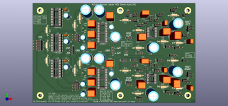
I've made some of the changes I've mentioned in my previous post, like:
Could you please take a look?
- Added GND vias to avoid islands
- Added power supply bypass capacitor (100 nF), between pins 4&7 of the I/V opamps/OTAs
- Increased hole size from 2.2 mm to 3.5 mm
- Changed some silkscreen text positions
Could you please take a look?
Attachments

Hi
Regarding jumper
Performance comment was generic. For your first pcb as a prototype board, your choice is fine.
Regarding decoupling
My comment only applies to 5534 op amp, a 100nF is ok.
The digital chips don’t need a 10uF paralleled to a 100n. 100n is enough.
Regarding ground.
Your vias looks ok, don’t hesitate to place clusters of vias as you did here to build the ‘bridge’ over the track.

Add don forget to run Kicad DRC to check for errors !
rgds.
Regarding jumper
Performance comment was generic. For your first pcb as a prototype board, your choice is fine.
Regarding decoupling
My comment only applies to 5534 op amp, a 100nF is ok.
The digital chips don’t need a 10uF paralleled to a 100n. 100n is enough.
Regarding ground.
Your vias looks ok, don’t hesitate to place clusters of vias as you did here to build the ‘bridge’ over the track.
Add don forget to run Kicad DRC to check for errors !
rgds.
Hi,
Do you have additional suggestions for improvement, or I can order the board like it is right now?
Regards,
Danny
I think I'm going to leave those capacitors, though they may be a bit overkill. I don't see any reason to remove them now that I have them already placed.Regarding decoupling
My comment only applies to 5534 op amp, a 100nF is ok.
The digital chips don’t need a 10uF paralleled to a 100n. 100n is enough.
Everything seems fine on DRC.Add don forget to run Kicad DRC to check for errors !
Do you have additional suggestions for improvement, or I can order the board like it is right now?
Regards,
Danny
- Home
- Source & Line
- Digital Line Level
- Digital noise/interference on the left channel