Hello, Hans! I need your help! That's why I assembled the amplifier. And in the process of setting up the currents, I had a short circuit... The Mje15031 q128 transistor and two 1r00f r79 r80 resistors near the nec 12v relay burned out. Hans, what is the Q128 transistor responsible for? And 1r00f resistors?So you want to replace U1 with a LT1097.
This one or the OPA227 is the chip that should be used for U1 on the voltage gain board.
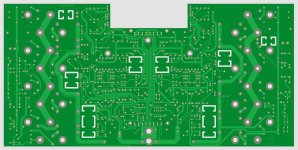
I have no idea what this 16 pin opamp may be, are you sure you are looking at the right PCB ?
Hans
Attachments
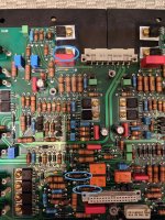

Hi,Hello, Hans! I need your help! That's why I assembled the amplifier. And in the process of setting up the currents, I had a short circuit... The Mje15031 q128 transistor and two 1r00f r79 r80 resistors near the nec 12v relay burned out. Hans, what is the Q128 transistor responsible for? And 1r00f resistors?
I can see that your picture is showing a 300 series current gain board and I also see Q128 written on it.
However, Q128 doesn't show up in the 300 series circuit diagrams.
And R79 and R80 are two 10R base resistors to the end transistors.
Is this a Mark Levinson amp or a Proceed ?
When you have a proper circuit diagram, I could give you some answers.
Hans
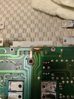
Hello, Hans. Yes, this is the ml 333 board, when installing the board, I closed the ground and phase on the switched-off amplifier 😬 in these places marked blue... There was a short circuit...I’ll try to answer your questions tomorrow.
Hand
Attachments

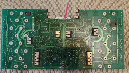
Here they are on the drawing of the board. I touched the 51000uf 160v capacitor bus with the board and shorted it to the amplifier housing...Я постараюсь ответить на ваши вопросы завтра.
Рука
Attachments
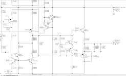
Yes, I also have this board layout image, but have a look at the current gain board circuit's diagram.
You won't find a Q128 and R79 and R80 are 10R and not 0R.
So what you have seems to use different numbers.
Hans
You won't find a Q128 and R79 and R80 are 10R and not 0R.
So what you have seems to use different numbers.
Hans
Attachments
Hans, as I understand it, the Mje15031 transistor is responsible for the 115v bias current. What are tf 20 resistors responsible for? Hans, I also burned a piece of land on the back of the board...Hi,
I can see that your picture is showing a 300 series current gain board and I also see Q128 written on it.
However, Q128 doesn't show up in the 300 series circuit diagrams.
And R79 and R80 are two 10R base resistors to the end transistors.
Is this a Mark Levinson amp or a Proceed ?
When you have a proper circuit diagram, I could give you some answers.
Hans
Attachments
I found your Q128, it's indeed the MJE15031 responsible for the negative regulated power supply, see circuit diagram below.
But for the 1R resistors R79 and R80 I can only find the base resistors for Q35 and Q36 that are 10R, so you may be wrong with the numbering.
Hans
But for the 1R resistors R79 and R80 I can only find the base resistors for Q35 and Q36 that are 10R, so you may be wrong with the numbering.
Hans
Attachments
Hello, Hans! I did not correctly specify the resistor numbers. These are two resistors r88 and r89. Hans, why do you think they could have burned out?Yes, I also have this board layout image, but have a look at the current gain board circuit's diagram.
You won't find a Q128 and R79 and R80 are 10R and not 0R.
So what you have seems to use different numbers.
Hans
Attachments
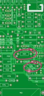
I'll tell you again what burned down. The dirt track burned down, I have already restored it. Two resistors burned out. Tf-20 R89 R88, transistor Mje15031 Q128.
Hi Mark levinson,
Those resistors load the output while in protect mode. So there is only one reason they might fail, and that is excessive power dissipation. Given that your negative regulator pass transistor also failed (probably excessive current & excessive dissipation), I would suspect a large negative DC offset.
The obvious troubleshooting direction would be to remove those resistors entirely, then power up the amp using a variac. Doing this will allow you to troubleshoot the amplifier without further damage. There is no need to bring the amplifier to full AC input voltage.
-Chris
Thank you, Chris! I'll do that.Hi Mark levinson,
Those resistors load the output while in protect mode. So there is only one reason they might fail, and that is excessive power dissipation. Given that your negative regulator pass transistor also failed (probably excessive current & excessive dissipation), I would suspect a large negative DC offset.
The obvious troubleshooting direction would be to remove those resistors entirely, then power up the amp using a variac. Doing this will allow you to troubleshoot the amplifier without further damage. There is no need to bring the amplifier to full AC input voltage.
-Chris
I have another problem, is different voltage applied to large capacitors in standby mode? I can't understand why this is happening. Is this a malfunction?
I'm not sure. I would have to examine the schematic in order to tell you that. If you have a lower voltage when not in standby, it is probably lower due to high current draw. So not a surprise. Remove the resistors, power up and see if you have the same fault. Check DC offset.
No, in Standby mode the large capacitors are fully charged, but bias current in the end stage is zero.Thank you, Chris! I'll do that.
I have another problem, is different voltage applied to large capacitors in standby mode? I can't understand why this is happening. Is this a malfunction?
When voltage in On mode is much lower, it means that bias current is much too high.
Hans
Hans, I took these measurements with discharged capacitors. The ml 27.5 has the same standby current on all large capacitors. 2.05V. And in this amplifier, for some reason, it is different... What on the vsmb board is responsible for supplying voltage to the capacitors? I know that the voltage comes out of p306 p305 p307 p312 p310 p311 and goes to the diode bridges further to the capacitors.Yes, either a large offset which normally would bring the amp into a fault mode or a more likely a defect relay K3 is the cause of burning those resistors.
Hans
Attachments
Hi Hans,
What you are suggesting would be a small voltage drop. It has already been established we have very high fault currents flowing in the output load resistors before muting is released. Without an input signal, this does mean a high DC offset. The failure of the negative voltage regulator transistor further supports this.
What you are suggesting would be a small voltage drop. It has already been established we have very high fault currents flowing in the output load resistors before muting is released. Without an input signal, this does mean a high DC offset. The failure of the negative voltage regulator transistor further supports this.
Hi Anatech,
The voltage regulator, who’s transistor was fried, is not feeding the current gain amp but only the voltage gain amp.
Whatever current is flowing in the end stage and in the two 1R resistors can never toast the Voltage regulator.
So the error in this case seems much more complex.
To start with the voltage gain amp has to be made fully functional in Standby mode, before the current gain amp can be added in the On mode.
Hans
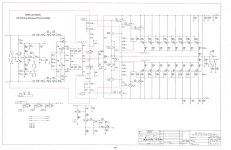
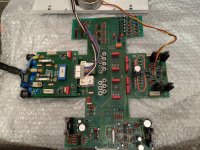
Very nice picture.Hans, I took these measurements with discharged capacitors. The ml 27.5 has the same standby current on all large capacitors. 2.05V. And in this amplifier, for some reason, it is different... What on the vsmb board is responsible for supplying voltage to the capacitors? I know that the voltage comes out of p306 p305 p307 p312 p310 p311 and goes to the diode bridges further to the capacitors.
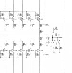
Here is the VSMB circuit diagram.
Hans
That's correct Hans, but a railed Vamp might draw enough current to cook the pass transistor. I'm not familiar with this particular amp from memory but I have worked on them. Therefore I am not 100% certain the Vamp can draw enough current to do that, but I know of some amps that certainly can. It may also be completely unrelated.
I agree that your Vamp needs to be working before the current gain stage can be used. A malfunctioning Vamp is exactly what is suspected here anyway. Removing the load allows you to run the current stage connected without disconnecting anything else. That's a plus in troubleshooting.
I agree that your Vamp needs to be working before the current gain stage can be used. A malfunctioning Vamp is exactly what is suspected here anyway. Removing the load allows you to run the current stage connected without disconnecting anything else. That's a plus in troubleshooting.
- Home
- Amplifiers
- Solid State
- Mark Levinson 333 in bad condition need your advice