Thanks Markw4, confirms my suspisions that there is possibly a DC component on the sharc pin, it could be charging an RC network on the fibre optic recieving module therefore introducing an offset to the spdif signal relative to ground and therefore clipping it. The time taken for the offset to 'appear' and then 'dissapear' would be dependant on the time constant of the RC network. Adding a film, C0G or X7R capacitor in series will block that DC offset.EDIT:
Regarding DC blocking for sharc chip SPDIF inputs, the following diagram can be found in: https://www.analog.com/media/en/technical-documentation/application-notes/ee.266.rev.2.08.07.pdf
It may not be there there is DC on the sharc input pin exactly. A careful reading of the sharc chip hardware data sheet might be needed to check for possible explanations. What could be another reason for DC blocking would be a case were the SPDIF source device was powered on, but the sharc chip was powered off. In that case the source device might apply a DC voltage to the sharc chip input which under the circumstances would exceed sharc Vdd (perhaps 0v, if unpowered). If that external voltage were then beyond the absolute maximum sharc chip input pin voltage limit, the sharc chip might damaged.
Of course with a TOSLINK receiver on the same board as the sharc hip and or when the TOSLINK receiver is powered by the sharc board, then the above condition might never be expected to occur. OTOH, if the TOSLINK receiver is on an external board not powered from the sharc board, then damage might occur if the system were powered on while the sharc board power connector had been left accidently disconnected following work on the system. Something like that, more or less.
Of course with a TOSLINK receiver on the same board as the sharc hip and or when the TOSLINK receiver is powered by the sharc board, then the above condition might never be expected to occur. OTOH, if the TOSLINK receiver is on an external board not powered from the sharc board, then damage might occur if the system were powered on while the sharc board power connector had been left accidently disconnected following work on the system. Something like that, more or less.
Okay, thank you. Again its important to check the datasheet for the actual device that will be used.
Also, regarding SPDIF interfacing circuits, there are a number of them out there. Here is another example sometimes seen (although sometimes the circuit is configured for LVCMOS voltage levels):

Also, regarding SPDIF interfacing circuits, there are a number of them out there. Here is another example sometimes seen (although sometimes the circuit is configured for LVCMOS voltage levels):
Last edited:
Sometimes just far easier and less time consuming to just try it or at least connect a DMM and check for DC.Again its important to check the datasheet for the actual device that will be used.
DC is hardly an issue here as TORX176 also operates at "TTL" logic levels. I would first check the Vcc on TORX176 as that is supposed to be powered from 5V, not 3.3V. So TORX176 may not be suited for ADSP21489 with 3.3V I/O. Another thing is that CSR8675 boards normally have different firmware for I2S output and SPDIF output. So the same board may not work with both output formats.
I think your white/purple wire pair is reasonably good for the spdif signal over Toslink, and you are unlikely have signal integrity issues with mere 14cm cable run even without any termination measures.
However, if I'm not mistaken, the TORX176 is a 5V device, and the I/O with the DSP that interfaces it is a 3V3 logic port. That mismatch may/may not be an issue. Since the TORX176 is quite weak in current sourcing at its output, it's unlikely to make any damages to the DSP, but the mismatching logic level could cause data errors. The signal current, albeit weak, that shoots through the input clamping diodes could also pollute the power rail inside the DSP. If you have not taken any measures against that logic level mismatch, perhaps try a 1k/2k resistor divider at the input of the DSP to scale down the level. Alternatively, if a more robust approach is preferred, scale down the logic level right at the output of TORX176, and buffer it with an SN74LVC1G125 operating at 3V3, before feeding into the white/purple wire pair.
However, if I'm not mistaken, the TORX176 is a 5V device, and the I/O with the DSP that interfaces it is a 3V3 logic port. That mismatch may/may not be an issue. Since the TORX176 is quite weak in current sourcing at its output, it's unlikely to make any damages to the DSP, but the mismatching logic level could cause data errors. The signal current, albeit weak, that shoots through the input clamping diodes could also pollute the power rail inside the DSP. If you have not taken any measures against that logic level mismatch, perhaps try a 1k/2k resistor divider at the input of the DSP to scale down the level. Alternatively, if a more robust approach is preferred, scale down the logic level right at the output of TORX176, and buffer it with an SN74LVC1G125 operating at 3V3, before feeding into the white/purple wire pair.
Here is another example sometimes seen
Few notes:
1) R1 is better to move after C1
2) R3 increase to 20-50k
3) 74HC04 will work, but it is better to replace it with 74LVC2GU04. Or similar - the main issue is "U".
4) Put a transformer at the input.
Yes, dsp distribute MCKSo, part of my question was about MCLK. Is there only one for the whole audio system and it is located on the DSP board?
Yes, I take power from dsp board VBUS and dsp is powered from usb, also tried powering torx and csr directly from that 'usb psu'I'm assuming that pin 1 on the fibre optic receiving module is connected drectly to a pin on the sharc dsp is that the case?
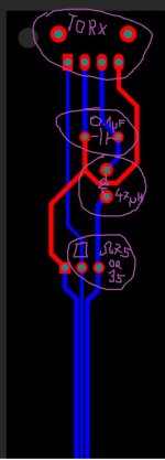
Was changing firmware myself, on i2s firmware was no sound at all or just noise, cant remember now.Another thing is that CSR8675 boards normally have different firmware for I2S output and SPDIF output. So the same board may not work with both output formats.
Not likely possible that csr with bad firmware and torx176 behave same way
I think that problem can be more trivial, remember that I am beginner with electronics
Is it possible that its related to GND? on board I made there is no ground plane, just thin traces.
Yes, torx is 5v, Im pretty sure that I read that sharc is 5v tolerant if thats good enough. BUT csr8675 is 3v3 (and takes 3.6-5v from psu), so it should work at least I guess.I think your white/purple wire pair is reasonably good for the spdif signal over Toslink, and you are unlikely have signal integrity issues with mere 14cm cable run even without any termination measures.
However, if I'm not mistaken, the TORX176 is a 5V device, and the I/O with the DSP that interfaces it is a 3V3 logic port. That mismatch may/may not be an issue. Since the TORX176 is quite weak in current sourcing at its output, it's unlikely to make any damages to the DSP, but the mismatching logic level could cause data errors. The signal current, albeit weak, that shoots through the input clamping diodes could also pollute the power rail inside the DSP. If you have not taken any measures against that logic level mismatch, perhaps try a 1k/2k resistor divider at the input of the DSP to scale down the level. Alternatively, if a more robust approach is preferred, scale down the logic level right at the output of TORX176, and buffer it with an SN74LVC1G125 operating at 3V3, before feeding into the white/purple wire pair.
Will try 1k/2k resistor and thinking about getting toslink receiver and will take 3v3 from known source now ie mouser, tme.. any recommendations?
Should I get 74LVC2GU04 also?
What kind of transformer?
I checked and there are no components added on dsp board for SDPIF INMay not be relevant but have you got a DC coupling capacitor in line on the shark dsp spdif input? On the ADAU14xx chips the spdif input is at half VCC and needs one to block the DC.
Also little update
Found DSP_BUS board layout, can see what components are used in 'original' aliexpress design, attached
Adapter board I use to connect everything looks like frankenstein now after all testing and ghetto mods, was no signal at all from both torx and csr.. and also shorted 3v3 from supply to ground of torx and ground to Vin.. I mixed the cables.
DSP still work with i2s fine, so maybe it survived. Will make new small adapter first so I can connect goldpins.
Attachments
Okay. Usually that would be considered suboptimal, all the more so if there is an MCLK isolator between the DSP and DAC boards. Its that a dac chip needs both a low-noise voltage reference and a low-noise time reference more so than any other part of the signal processing. Jitter/Phase-noise can best be minimized if using a good crystal clock located very near the dac chip. Also, Vref (aka AVCC), the voltage reference, should located very near the dac chip.dsp distribute MCK
With master clocks close to the dac chip, then a clock buffer chip (e.g. NB3L553-D) could be used to drive other devices needing a copy of the the system master clock. Also, using ultra low phase noise clock buffers can help keep crystal clocks loaded for best stability while maintaining low phase noise on all MCLK clock copies. If, say, for example, a clock buffer is used to drive a an MCLK isolator between the dac and DSP boards so as to provide the DSP board a copy of MCLK, then after isolated I2S is sent to the dac from the DSP board, a D-flip flop reclocker circuit can be used on the dac board to remove/attenuate any remaining jitter on I2S signals (although some people might feel in theory a little jitter shouldn't matter there, other people feel that a little I2S jitter can still introduce some noise effects into the dac chip). My own preference would be to reclock.
Last edited:
For dacs its usually considered that 4-layers is the minimum. Some people are now using 6-layers, since prices may be coming down for that option. Usually the top layer is for signals, and the 2nd layer (the one just below the top) a ground plane layer. 3rd layer might be power or another ground, and bottom layer could be for more signals....board I made there is no ground plane, just thin traces.
I will definitely go with power and gnd plane next time. Dont think Im ready for dac yet. Board I masę was for sięgnął distribution from DSP, as DSP board developer used non standard 2.0 raster headers. Quick and dirty, and first board I made. I ready somewhwre that I shouldnt worry much about 'slow' signals like i2c, i2s..Will improve over time
I2S is not slow. Its definitely RF. Perhaps consider that square waves have lots of odd harmonic frequencies which are related to edge risetime. Frequencies extending up into the hundreds of MHz are not unusual.
Slow/Fast - "it depends".
I2C can be up to 1MHz, (btw, there is I3C which is much faster).
I2S - up to a ~25-50MHz.
If compare with SATA, DDR, etc. - I2C and I2S are slow 🙂
Of course, even few megaherz with harmonics are fast enough to take care about PCB layout and layers stackup/
4-6 layers are good, but not always mandatory.
I2S can be ~25-50MHz square waves. You understand about Fourier? Time domain verses Frequency domain?
Maybe this will help: https://en.wikipedia.org/wiki/Square_wave#:~:text=The ideal square wave contains,wave is the Gibbs phenomenon.
At 24/192 PCM, BCLK is ~12Mhz. Third harmonic is at 36MHz, 5th is at 60MHz. Starting to look like a square wave, but not really all that square yet.
Looks about like this:

So maybe not well up into the GHz region, but hundreds of MHz is quite possible with I2S.
The problem is that you also have analog audio running through opamps in the same environment. And you want -120dB SNR, ultra low distortion, etc.? The transistors in your opamap are going to demodulate that RF and then intermodulate it with your audio. So you have to control where the RF fields go, how they are contained, etc.
Maybe this will help: https://en.wikipedia.org/wiki/Square_wave#:~:text=The ideal square wave contains,wave is the Gibbs phenomenon.
At 24/192 PCM, BCLK is ~12Mhz. Third harmonic is at 36MHz, 5th is at 60MHz. Starting to look like a square wave, but not really all that square yet.
Looks about like this:
So maybe not well up into the GHz region, but hundreds of MHz is quite possible with I2S.
The problem is that you also have analog audio running through opamps in the same environment. And you want -120dB SNR, ultra low distortion, etc.? The transistors in your opamap are going to demodulate that RF and then intermodulate it with your audio. So you have to control where the RF fields go, how they are contained, etc.
Last edited:
Ok, so update.
I took another another PCB, soldered core board to my PCB this time. Spdif is back on.. so are clicks and pops after couple mins, as before.
Tested with csr only and decided I will focus on this for now.
So what to components I should add for csr connection?
75ohm resistor + 0.1uF cap on sięgnął line?
Anything else?
Also will try to power digital part from power bank.
Power bank may not be wonderful in some respects. Probable internal SMPS to regulate power bank output voltage.
75R SPDIF load resistor is to control transmission line reflections.
Regarding your DSP chip and SPDIF interfacing, the ADSP-21489 evaluation board shows an example of SPDIF interfacing on page 94 of the document at: https://www.analog.com/media/cn/tec...ser-guides/ADSP-21489_ezboard_man_rev.1.1.pdf Don't know to what extent that applies to ADSP_214XX in general.
For ADSP-21467, absolute maximum voltages are shown on page 22 of the document at: https://www.analog.com/media/en/technical-documentation/data-sheets/adsp-21467_21469.pdf According to that the input voltage maximum range is: Input Voltage –0.3 V to +3.6 V ...Obviously a 5v input would be way out of spec.
Nice find Mark, didnt think to look for a dev board. Think should be same for whole ADSP_214XX series, I have ADSP-21489 anyway.
So torx176 output is 5v? Thought there are some standards.. i2s can be also various voltage?
I did dig a bit and found circuit they use for spdif(coax) in from your EZ board pdf
Example spdif out for csr8675 and ratings
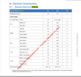
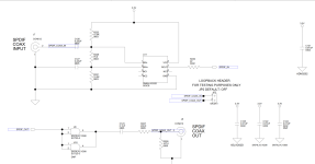
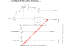
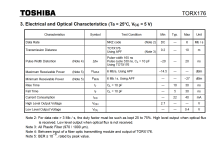
So torx176 output is 5v? Thought there are some standards.. i2s can be also various voltage?
I did dig a bit and found circuit they use for spdif(coax) in from your EZ board pdf
Example spdif out for csr8675 and ratings


Last edited:
I2S bus spec at: https://www.sparkfun.com/datasheets/BreakoutBoards/I2SBUS.pdf
Voltage levels on page 5.
Some info on logic voltage levels: https://www.sparkfun.com/datasheets/BreakoutBoards/I2SBUS.pdf
Also: https://www.renesas.com/us/en/document/apn/124-33v-logic-characteristics
Voltage levels on page 5.
Some info on logic voltage levels: https://www.sparkfun.com/datasheets/BreakoutBoards/I2SBUS.pdf
Also: https://www.renesas.com/us/en/document/apn/124-33v-logic-characteristics
Last edited:
- Home
- Source & Line
- Digital Source
- S/PDIF input problem