
Use R2 to set the current draw of the amplifier to about 1A. The BD139 can get very hot with a small R2 value.
Check the correct inclusion (pinout) bc559.
Adjust the level of the signal (music) at the input of the amplifier. At high levels, the sound may be distorted.
Check the correct inclusion (pinout) bc559.
Adjust the level of the signal (music) at the input of the amplifier. At high levels, the sound may be distorted.
Last edited:
thanks both!
Mooly:
When R2 is turned somewhere mid-way (not hot BD139 distorted sound):
I double checked bc559 its seems good
Mooly:
When R2 is turned all the way (hot BD139 + clean sound):Check the voltage across the 2k2 across the base/emitter of TR1 and make sure it reaches around 0.65 volts (approx figure) when you turn the pot. Also check the B/E voltage across TR2
- TR1 voltage across b-e seems super low - 0.025v
- TR2 B-Ground, E-Ground are both ~9v, B-E is around 0.6V
When R2 is turned somewhere mid-way (not hot BD139 distorted sound):
- TR1 voltage across b-e seems still super low, can't seem to measure
- TR2 B-Ground, E-Ground are both ~8v, B-E is around 2-6V AC
The source level is pretty high but i've tested it with my phone with lowering the volume which gave the same distorted soundUse R2 to set the current draw of the amplifier to about 1A. The BD139 can get very hot with a small R2 value.
Check the correct inclusion (pinout) bc559.
Adjust the level of the signal (music) at the input of the amplifier. At high levels, the sound may be distorted.
I double checked bc559 its seems good
TR1 voltage across b-e seems super low - 0.025v
Check that TR1 is OK and has not got a near short across B and E. Make sure that the 2k2 is really a 2k2 and not a 2.2 or 22 ohm by mistake.
Check all transistors and resistors. Check the correctness (polarity) of the electrolytics and the absence of a breakdown.Check if the connections are correct. Measure the voltages at the test points (as in the figure). The load connection scheme is different.
Attachments
Last edited:
thanks again! this is super helpful..
@Mooly - I think you are right, there seems to be a short on Tr1
My transistors weren't insulated to the heatsink in my first tests and may have shorted? hmm.. I've never used these kind of metal cased transistors on a heatsink before, they are now all with a ceramic screw+washer insulators.
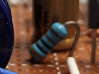
The resistor I have across TR1 B/E looks like the picture below - I am not 100% sure but with the help of a colour calculator it should be a 2k, hopefully i am seeing the colours correctly.
Also @OldDIY I agree.. I may need to do a bit of a fresh check across the whole board once I replace the parts that may be causing the issues..
I am thinking to get new TR1/TR2 transistors and 2k2 next week.
@Mooly - I think you are right, there seems to be a short on Tr1
My transistors weren't insulated to the heatsink in my first tests and may have shorted? hmm.. I've never used these kind of metal cased transistors on a heatsink before, they are now all with a ceramic screw+washer insulators.
The resistor I have across TR1 B/E looks like the picture below - I am not 100% sure but with the help of a colour calculator it should be a 2k, hopefully i am seeing the colours correctly.
Also @OldDIY I agree.. I may need to do a bit of a fresh check across the whole board once I replace the parts that may be causing the issues..
I am thinking to get new TR1/TR2 transistors and 2k2 next week.
Attachments
A friend that I had guided by telephone years ago to assemble a JLH had made the exact same mistake, I had not thought for a minute that he could assemble them without insulators 🤪thanks again! this is super helpful..
@Mooly - I think you are right, there seems to be a short on Tr1
My transistors weren't insulated to the heatsink in my first tests and may have shorted? hmm.. I've never used these kind of metal cased transistors on a heatsink before, they are now all with a ceramic screw+washer insulators.
The resistor I have across TR1 B/E looks like the picture below - I am not 100% sure but with the help of a colour calculator it should be a 2k, hopefully i am seeing the colours correctly.
Also @OldDIY I agree.. I may need to do a bit of a fresh check across the whole board once I replace the parts that may be causing the issues..
I am thinking to get new TR1/TR2 transistors and 2k2 next week.
;-)Hey all, my JLH is showing some initial signs of life but with some strange behaviours and I need some ideas 🙂
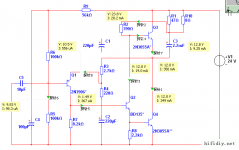
It is pretty much following the JLH69 schematics with:
Transistors: BC559, BD139 and BD249C
Power is right now an 18v / 6A laptop SMPS and my speakers are 8Ω
I have hooked everything up, set the Vx to half (9v) and started to test out with some music source.
If you look at the attached JLH circuit part names I have an 100Ω for R1 and 1K pot for R2.
I only manage to get clean sound when R2 is turned all the way to one end and while turning it towards the other direction the sound gets distorted pretty badly.
At the same time whats really weird is:
- with R2 all the way with the clean sound TR3 (BD139) and R1 (100Ω) get really hot but the two Transistors attached to the heatsink stay cold.
- with R2 all the way to the other end TR3 and R1 are not as hot and the heatsink transistors are still cold.
Any ideas or suggestions would be much appreciated!
I would remove C1. Without C1 it will sound much better: cleaner, more homogenic.
And set R1 and R2 as one trimmer to be able to set the optimum quiescent current. Later I would replace by an power-resistor - if the load should be too high for e little trimmer.
My advice is not to remove C1, this is part of the bootstrap loading on BD139 collector.
Bootstraping the Vas transistor was a common approach used in amplifiers dating from the 1960 decade. You should take that as an article of faith if you don't understand JLH 's reason for using this.
Bootstraping the Vas transistor was a common approach used in amplifiers dating from the 1960 decade. You should take that as an article of faith if you don't understand JLH 's reason for using this.
I would remove C1. Without C1 it will sound much better: cleaner, more homogenic.
I do not advise you to remove C1 from the circuit, because the gain of the driver transistor will weaken and the depth of the negative feedback becomes less than the required level in order to call this amplifier ultra-linear, of course for its 1969 year ...
about "cleaner" and "more homogenic" - this is some kind of deception, because without C1 the transient response begins to have a different slope of the fronts, in fact it turns out rather dirty and heterogeneous ...
Last edited:
If you look closely at the attachment in post 8485 above, you'll see that C3 (the output cap) takes the place of C1 by using the + rail as the speaker return. Kinda weird because feedback still goes to the negative rail which is not ground anymore, or is it ?
The negative rail doesn't have to be ground but as drawn it is the 'reference' rail that the input voltage and feedback use as a common point. Taking the load to the plus rail will work but anything other than a zero impedance supply rail will cause the output to be influenced by the rail (such as ripple and modulation by another channel). So not great as it stands.
why do that?f you look closely at the attachment in post 8485 above
suitable for portable radio when sound quality is not essential...Kinda weird because feedback still goes to the negative rail which is not ground anymore, or is it ?
;-)
Should be possible too:
R1: V+ to base of Tr2
R2: emitter - base of Tr2
The sound should get more "smack", thicker colours, more body.
NO C1, because...
Should be possible too:
R1: V+ to base of Tr2
R2: emitter - base of Tr2
The sound should get more "smack", thicker colours, more body.
NO C1, because...
;-)in fact it turns out rather dirty and heterogeneous ...
it's hard to comment on freak solutions, especially when the ears become the main tool for determining quality...
 Some posts removed. Keep it civil, or we may need to start giving timeouts.
Just to expand on this the bootstrap involving C1 increases the a.c. impedance of the load seen at the collector of the BD139 transistor which means that will have to pass more collector current to generate a greater voltage drop across the impedance of the load.I do not advise you to remove C1 from the circuit, because the gain of the driver transistor will weaken and the depth of the negative feedback becomes less than the required level in order to call this amplifier ultra-linear, of course for its 1969 year ...
about "cleaner" and "more homogenic" - this is some kind of deception, because without C1 the transient response begins to have a different slope of the fronts, in fact it turns out rather dirty and heterogeneous ...
It is necessary to get the right level of operating current for the BD139 by studying a graph where collector current is plotted on the vertical axis and collector to emitter voltages are plotted on the horizontal. A line representing the load is drawn between selected levels between two points between each axis.
The characteristics of transistors have a curved characteristic if the levels are not correct then the Q point which crossed the graph for the particular transistor is too high the result will be a clipped signal.
The approach to resolving this question is to download the datasheet for BC639 and look at the graph for static characteristics. These are low power versions of BD139 with max IC current of 100 m.a. with less heat dissipation characteristics. The values of the resistors in between the collector of BD139 and the supply rail are the dc load which will be boosted by the bootstrap capacitor C1.
The reason for this is the circuit has two common emitter amplifier stages each of which invert the phase of the output for each. Two negative phases result in a positive phase input from the output connection to the loudspeaker via C1 when applied to collector of BD139. Bootstrapping involves the use of positive feedback to increase the ac impedance of the BD139 collector load.
There is no static graph for BD139 in the datasheet
It's right.The reason for this is the circuit has two common emitter amplifier stages each of which invert the phase of the output for each.
In this case, the input first transistor (IS) amplifies at the level of 6.3dB, and the second transistor (VAS) amplifies 42dB (open loop).
If we remove the capacitor, then the first transistor adds +1dB,, but the gain of the second transistor drops to 36dB.
It is easy to calculate the resulting feedback depth necessary to reduce distortion and increase the linearity of the gain stages.
The problem with basic calculations like this is that these are small signal figures. Applying the required feedback will give a low-level distortion figrue which would be expected, but not large signal. The Linsley-Hood circuit works by having the output transistors oppose, to largely cancel second harmonic distortion, but distortions increase at high output levels which has to be measured, or calculated on the basis of transistor parameters at the appropriate bias points. Many transistors of the older gen have quite strongly degrading gains with increasing current, and conversely increasing at lower currents until they pass the peak, so while a lot of distortion cancellation occurs, it is not perfect. Better results would in principle be achieved with the modern "linear gain" devices.
I have the Wireless World publication "High Fidelity Designs published in 1974 which includes an addendum to the 1969 article in letters to the editor. In this JLH attributed an apparent fall off frequency in figures 4 and 5 - this when measured with better equipment. The second of these items showed THD of 0.05% ruler flat from Hz up to 20kHz. Distortion at the low end approached 0.15% getting down close to 50 Hz in frequency response. The standing current was 1.2A for 8 Ohm loads and 0.9 A for 15 Ohm loads which were quite common for speaker loads in 1969.The problem with basic calculations like this is that these are small signal figures. Applying the required feedback will give a low-level distortion figrue which would be expected, but not large signal. The Linsley-Hood circuit works by having the output transistors oppose, to largely cancel second harmonic distortion, but distortions increase at high output levels which has to be measured, or calculated on the basis of transistor parameters at the appropriate bias points. Many transistors of the older gen have quite strongly degrading gains with increasing current, and conversely increasing at lower currents until they pass the peak, so while a lot of distortion cancellation occurs, it is not perfect. Better results would in principle be achieved with the modern "linear gain" devices.
The output transistors chosen for this circuit had 4MHz unity gain capability. If 2N3055's with lower unity gain frequency and lower Hfe were substituted the same level of performance could be achieved by replacing 2N1611 with 2N1711. There was some need to match the output transistors for current gain however MJL21194 transistors are designed to be a good match for MJL21193 a point I have raised before and to achieve this sort of claimed result MJL21194 transistors should be a reasonably close match for others in the same production batch.
At the levels of operating currents for this design the unity gain frequency for these is in excess of 7 MHz so there should be no problem. One should look at the datasheet for BD139 and that for 2N1711 to draw comparisons for such as collector to base capacitance etc. In general lower capacitance in the last regard should be better because that capacitance will be amplified and presented as a load at the base - the phenomenon of Early effect which was well enough understood at the time - a limiting factor mentioned with the Bailey Class AB circuit in the same publication.
Samuel Groner looked at this problem in his paper "Audio Power Amplifier Design Handbook" by Douglas Self dated February 13, 2011 and came up with a rule of thumb method for a figure of merit for a VAS transistor determined by hFE. VA What was actually used was hFE. Vceo. 11 transistors were subject to testing - see this link https://www.nanovolt.ch/resources/power_amplifiers/pdf/audio_power_amp_design_comments.pdf.
Note as already mentioned low collector to base capacitance is covered in the first paragraph on page 27.
Silicon Chip magazine published a version of the Blamless amplifier due to Self in December 2021. In this they measured the distortion with various output transistors, various drivers, and various Vas types. The last category included KSC3505DS, BF469, BD139, and MPSA42. The preferred device was KSC3503DS, BF469 performed to the same level, BD139 had slightly elevated distortion but noted these were offered by several manufacturing sources. MPSA42 tended to result in more negative rail sticking. The supply rail voltages for this project are +/- 32V although some tests were done with a 25-0-25 Volt ac transformer. BF469 is sold by Jaycar in Australia these will be from less well known manufacturers so if one has some old stock of these it would be best to stick with these.
- Home
- Amplifiers
- Solid State
- JLH 10 Watt class A amplifier