I've been having a look at Nelson Pass's A40 Class A design, that originally appeared in Audio magazine in the late 70's. I have done an update of the design that eliminates the tantalum capacitors and the need for the unobtainium Llambda power Darlingtons originally used in the design. This comes at the expense of discrete Darlingtons, but the ability to choose zippy updated bipolar driver and output devices, as well as being able to optimize the driver termination resistors may make up for the added complexity. All the parts should be available from the usual suspects. I'll post a prelim schematic when things quiet down for me a bit (3-5 other projects in the works). Of course I'm posting with the full realization that this is not strictly a Pass design any more, as so many aspects of the design have been changed.

My take on it is not quite as simple, but I think it addresses some of the frustrations would-be builders would have with the design using currently available parts. Just about all the semiconductors called out in the original design are obsolete. I also chose a different scheme to implement DC unity gain that gets rid of the tantalum capacitor and substitutes a high quality film cap instead.
I've been chipping away at the preliminary schematic for this updated circuit, and here are the changes I've been making so far:
1) Darlington for upper VAS stage
2) Alternate feedback circuit for unity gain DC feedback using film cap instead of tantalum
3) Discrete vs. integrated output Darlingtons to avoid having to use obsolete integrated devices
4) Current mirror loading for input diff pair
5) Use of small-signal N-channel Mosfets for input diff pair to enable 2)
6) use of currently available depletion mode mosfet instead of obsolete jfet for setting input differential stage and VAS bias
7) biasing using GaAsP red LED (~1.6 VDC @ 10 mA bias)
8) protection for mosfet diff input to avoid static damage
Devices considered so far - KSA992, KSC1845, TTA004B, TTC004B, ZVN3306A, BSS159, 2SA1386, 2SC3519
I may entertain suggestions for replacement of the last 2 devices for ones with similar ft and higher power dissipation capability.
Obviously, the resulting circuit is going to be more complex than the original A40, which was astonishingly simple for what it did. I may sling something together in PSpice with the models I have available to me to determine if the extra complexity is worth it. Having said that, though, all the parts I've mentioned so far are currently available at Digikey without a lot of roaring and screaming. When I get around to futzing with the reference designators and values for the circuit I have going, I will post it.
Not so fast, Newark has a few and NJsemi has a few thousand in stock. Try http://njsemi.com/parts/PMD16K100 and http://www.njsemi.com/parts/PMD17K100.... unobtainium Llambda power Darlingtons originally used in the design...
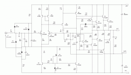
I'm continuing anyway, as those devices won't be around forever. I also want to see what the combo of 100MHz ft driver and 30 MHz ft output will do to the design. I'm attaching a preliminary schematic. It has a lot of the extra doodads that subsequent pundits have added to improve designs (most notably, some ideas from Dale Self), so it's definitely not as stunningly simple as the original A40. I plan to load the design into PSpice using whatever appropriate models I can find to see if the extra complexity is worth it. If not, some of the extra doodads will get stripped out. As a rock to stand on, though, the mosfet diff input will stay, and the discrete Darlingtons in the output will stay.
Indra, I'm willing to bet that the New Jersey Semi PMDs will be different compared to the original Llambda part. Just because it says "PMD" on the outside doesn't mean that the actual guts inside will be an exact equivalent to the original part.
Indra, I'm willing to bet that the New Jersey Semi PMDs will be different compared to the original Llambda part. Just because it says "PMD" on the outside doesn't mean that the actual guts inside will be an exact equivalent to the original part.
Attachments
Last edited:
Just to set some other things in stone as well, I'm proceeding with this alternate design for my own reasons. I'm nobody's unpaid remote control design engineer and and tech. I've been designing and building amps with varying degrees of success for 45 years.
If you want to do a closer variant of the A40 with currently available devices, I would just cut the Gordian knot and substitute some modern TO-92 devices - MPSA06/MPSA56 or 2N5401/2N5551 come to mind. These, combined with the Darlington outputs of your choice will get you something simple that will work without a whole lot of agonizing and messing around. At the cost of a little extra nitpicky complexity, you could substitute a PNP ring-of-two current source for the jfet used in the original design that sets the current for the diff stage and the lower VAS transistor.The ring-of two source would be more predictable.
Last edited:
wrenchone, my remark was not about your choice, rather about other members who wanted to make the A40 being deterred by your unobtainium statement. The A40 has a special place in my view being the first NP amp I made in the 80s, works without a hitch the first time.... I'm nobody's unpaid remote control design engineer and and tech. ...
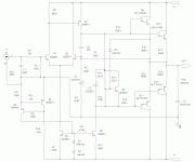
Well, that's still my view - I'm into this project for my reasons, and after all, I'm also doing all the work. Anyway, a bit back, I teased a simpler update of the A40 using currently available devices. Attached is my suggestion for same. As I mentioned before, I replaced the jfet current source with a ring-of two bipolar current source, which will be more predictable than the original jfet current source, though it may have been NP's intention that the absolute value of the current source didn't matter all that much, as all it was doing was feeding the diodes that biased the current source for the diff pair tail and the bottom half of the VAS. I used some rugged 30A Darlington devices for the outputs that are currently available in TO-3 flavor from Digi-Key (they're pricey, though). If one wants to sub Kablambda copies instead, one can...
Attachments
I looked at Digi-Key for 2N5401 and 2N5551, and I just about had heart stoppage as Digi-Key lists them as obsolete. However, Mouser came to the rescue with parts from several sources. Mouser also has the hunky 30A Onsemi Darlingtons, though still pricey.
Last edited:
Don't know if it is intentional or not but your V2A does not feature the input impedance bootstrap of the original A40.
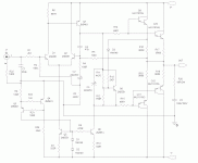
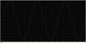
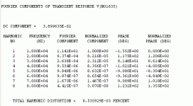
OK, I ran a PSpice simulation on the schematic in post 13 using 0.5V excitation and an 8 ohm load. With the original schematic values, the output offset was ~50 mV, and the THD was around 0.0087%, most of the content being 2nd and 3rd harmonic. This is not a horrible place to be, but I generally like to see the input diff stage balanced a little better than that. This is one reason why I often use a small-signal mosfet pair for the diff input stage. The input bias current is extremely low, so I don't have to jump through hoops like NP did to try and equalize the DC impedance on both inputs of the diff amp. I find, at least in simulation, the the closer the input diff pair is balanced, the better the distortion figure. I tried scaling R5 from 10k down to 8.66K, with R4 and R3 also scaled down proportionately. I got a little better output offset, and the 5th and 7th harmonic content also went down some. Attached is the sim schematic with all the bias values, the output waveform, and the sim distortion profile. I will wait until I get back to work on Monday to try and sim the more complex schematic, as my work copy of PSpice has a lot more models to choose from than the downrev version I'm running here at home. BTW, I used 2N6284 and 2N6287 as output devices in the sim, as those are the models that were readily available.These are probably not a bad choice for a real version of this amp, as they are rugged and not that hard to find.
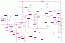
When I get back to work, I may try a sim of the schematic in post 13 using ZVN3306A mosfet inputs and discrete Darlington outputs - a little more complex than the original A40, but still readily buildable with parts available right now. As a bonus, the input mosfet diff stage will allow me to use my favorite DC unity gain scheme.
When I get back to work, I may try a sim of the schematic in post 13 using ZVN3306A mosfet inputs and discrete Darlington outputs - a little more complex than the original A40, but still readily buildable with parts available right now. As a bonus, the input mosfet diff stage will allow me to use my favorite DC unity gain scheme.
Attachments
Last edited:
Congratulations @wrenchone on a great looking, super fun project! Wishing you tremendous success.
Would you also consider NJFETs for the input differential pair? They have negligible input bias current and usually have lower internal capacitances than discrete TO-92 MOSFETs. Looks like in this design, a JFET would need Vdsmax > (32V supply + (32V / closed_loop_gain)) so for a closed loop gain of 11X, that's a Vdsmax of 35V. Nelson Pass said in his BAF 2022 talk that he's measured NJFETs part number "J113" and found they work all the way up to 70V.
Possibly maybe MJL3281 / MJL1302 for the darlington-using-discretes concept? They have awesome specs and superb SOA. Bob Cordell measured them and fitted SPICE models himself, which are freely downloadable from his website.
NFETS may be a possibility, but I would probably end up cascoding the ones I would most like to use. The Onsemi devices are also a possibility for discrete Darlingtons, and they were some of the ones I had in the back of my mind, along with the Sanken devices I called out in my earlier, more complex schematic. Unfortunately, adding libraries to my PSpice is complicated by the fact that it's intimately wrapped with Orcad capture. Once I figure out how to do it, the world will be my oyster...
I had a look at the devices I've recommended or simulated for output integrated Darlintons so far, these being the 2N6284, 2N6287, MJ11015 and MJ11016. NP originally chose the Llambda integrated Darlingtons for the A40 because of the low value of bias resistor for the first driver stage, ~25 ohms, but If you look at the devices I mentioned above, they don't look all that bad either, with ~50 ohm bias resistor for the 2N6284/87, and ~40 ohms for the MJ11015/016.The Onsemi TIP141/147 also don't look too bad, with ~40 ohms for the first stage bias resistor. However, the ST version of the parts fares worse.
Last edited:
I could envision a design using 3 pieces each of onsemi TIP141 and TIP147 to spread out the load, as it is not as robust a device as some of the others I have mentioned. You possibly might want to kick the emitter resistors up to about 0.75 ohms each, to spread out the dissipation. When you're playing the SOA game with weaker devices, there's safety in numbers... Unfortunately, the onsemi TIP141/147s appear to be at end of life, and all the people building AB100s appear to have sucked up most of the available stock from the two main on-line distributors. The variety available at Newark (Multicomp) is an abomination, with bias resistors orders of magnitude higher than they should be - stay away from that one at all costs.
Last edited:
TIP142G/TIP147G from OnSemi are still available, 142G on backorder at mouser, OnSemi has both marked as 'active'. In fact i'm updating my A40 with these outputs. My old version has the MJ11015/16. I'll be following this one for sure, A40 is a fantastic amp. I used KSC1009 for the inputs and elseware in the original circuit, MPSA93 for Q4. LM334 for the current source. Sounded pretty good to my untrained ears.
Last edited:
- Home
- Amplifiers
- Pass Labs
- Updated Pass A40 Design