Improperly designed power amp units where output power transistors with 30-60MHz are in use as mentioned in post #1 under
https://www.diyaudio.com/community/...amilies-for-audio-power-output-stages.147656/
may degenerate into an RF oscillator - unfortunately often only temporarily (removing or moving of only a single cinch-wire or mains power cord or move the amp device of any few cm lets abruptly break off the unwanted oscillation).
Main reason therefore is a bad layout choice of the conductor tracks - consequence is, that several parasitic capacities are additional present.
Most audio engineers still believe that with regard to human hearing from 20Hz to 20KHz, the design of audio power amplifiers is completely uncritical (compared to power amplifiers for RF/HF applications) and checking the frequency response of audio power amplifiers up to 100 MHz is complete nonsense from the view of those engineers.
I don't think so.
I claim, an examination of those frequency area below and a bit above ft of power output transistors is definitely necessary - i. e. between 0,5 MHz and 100MHz, if ft from power Transistor is 60MHz.
Which is well very far away of 20 KHz.
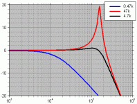
Only then can one clearly see whether there is a tendency to oscillate or not. If there is a tendency to oscillate, the plot looks basically like those from the attached image (red curve) - but the peak is mostly between 1MHz and 10MHz.
If there is full level RF oscillation or if there is an undesired oscillator function immediately (recognizable by the immediate destroy of the output power transistors due occur of max quiescent current value that be supplied by the power supply), this can only be proven with a power supply with integrated current limiting unit (one suspects at first glance faulty pot in the vbe multiplier stage - go to post 14 under
https://www.diyaudio.com/community/threads/differences-between-various-vbe-multipliers.117047/)
With any few amplifier models that I had on my desk because oscillation issues, I was able to find out the reason with help of the CAD program CIRCUITMAKER. These were the amp models I remember well:
1) Meracus Onesta Integrated Amplifier
http://ftbw.de/xp/amplifier-xp/meracus-onesta-v1.html
The device oscillated sporadically to around 3 MHz with nearly full voltage swing (without speakers and 1K load) also depending on the routing of external connecting like cinch cables) - accompanied by rapid heating of the output transistors BD911/912 (three pairs in parallel mode).
My repair was supposed to be the fourth attempt - this amplifier device had actually been abandoned from the owner.
In the simulation of this circuit topology the frequency response looked smooth up to around 400KHz and dropped off at around 6db/oct. without anomalies up to 100 MHz
Parasitic capacities due to conductor tracks running in parallel were initially not taken into account while first circuit design from the this German manufacturer. As is well known, a capacitance between the output and the inverting input (in parallel with the NFB resistor) is critical, which was not planned or taken into account while circuit design.
Due to the parallel PCB routing on both component and solder sides, a capacitance of about 70pF was created (noted by measuring after de-solder several resistors and caps around the NFB loop).
After introducing this capacitor into the circuit in the simulation (CAD-program), the oscillation was also present here - slightly deviating in frequency and level in opposite to those from real live (according my own oscillographic measurement).
The frequency response measurement looked basically like the last diagram on the third to last page under
https://hifiakademie.de/pdf/phono.pdf?si=google
however, the peak before the drop was around 2.5-3MHz.
I increased the capacitance in the circuit under simulation to 220pF, which made the peak even more pronounced, and then changed the values of all present compensation capacitors so that a flawless "roll-off" between 1MHz and 100MHz was occur (effortful work and many sessions on my personal computer).
After introduction of new capacitors in the "ONESTA" itself with the values from the simulation and the 150pF capacitor parallel to the NFB resistor (= 220pF ./. 70pF), flawless operating without any RF artefacts resp. ring-ring effects was also recorded in real live, which is still the case until now (about 15-18 years ago).
2) Luxman L190
integrated bass-treble control in the NFB loop of power amp section (and passive preamp consisting of source resp. input selector and volume control) - go to
https://elektrotanya.com/luxman_l-190a.pdf/download.html
Perfect function in the middle position of treble control pot - degenerates into an oscillator when the treble control is turned down, the occurred oscillation level being so low that the output stage transistors are not destroyed.
Frequency of ring-ring around 100-200KHz.
Power amp not unity gain stable (same phenomenon as on op amps, not unity gain stable without external compensation). Regardless of whether speakers are connected or not.
The problem was not eliminated because in the currently application the trebles of the loudspeakers used were usually turned up further (full range driver in use without dome tweeter).
3) Philips F4215
https://www.hifiengine.com/man…brary/philips/f4215.shtml
Same observations as on Luxman's L190, but maximum level and destruction of both STK chips.
Correct working amplifier channels without RF oscillation designed with the help of the mentioned CAD program - after doing this no longer RF oscillation even in min-position of treble control pot. Unfortunately I don't have the details anymore. As I remember right, main effort was the creating of a unity gain stable power amp unit.
4) Horch 3.0S
https://www.diyaudio.com/commu...er-output-devices.379808/
Depending on the location, the fuse sometimes but not always blows - even without speakers connected.
Most likely unwanted high level RF oscillation as well. Still has to be tested with a laboratory power supply and current limitation.
In general, it has always bothered me that there are no measurements for home audio amplifier models up to at least 100 MHz and I cannot make any myself to prove whether the peak before the final frequency response drop is missing or not - the latter would always indicate that the phase reserve is too low - see basic description under
https://bilder.buecher.de/zusa…20871/20871854_lese_1.pdf
A low pass filtered square wave form at the amplifier output as seen under
https://www.amplifier.cd/Verstaerker/verstaerker/images/rechteck_10kHz.jpg
and numerous under
http://saba-forum.dl2jas.com/index.php/Thread/8271-square-wave-behavior-of-hi-fi-amplifiers/
is no guarantee that no oscillation or undesired ringing can occur - but a smooth roll-off (i.e. without a preceding peak in the upper range befor falling) in a frequency response measurement up to 100MHz is a clear evidence of this.
To carry out this measurement one need an RF-capable broadband noise generator and the possibility of such a frequency response measurement display. Furthermore, all filter capacitors must be removed outside of the NFB loop - mainly the input capacitor for limiting the slew rate and limiting the upper cut-off frequency - otherwise I get not helpful results and looks like those under
https://www.amplifier.cd/Verst…ages/gain_db_normiert.gif
Does anyone have experience with this kind of measurement on audio amplifiers ?
Which measurement could alternatively (to the frequency response up to 100MHz) to be made to estimate the risk of unwanted RF ring-ring ?
Many thanks for hints.
P.S.: this threads don't provide the appropriate information:
https://www.diyaudio.com/community/threads/amplifier-oscillations.3767/
https://www.diyaudio.com/community/threads/audible-or-noticeable-symptoms-of-oscillation.73724/
https://www.diyaudio.com/community/...il-override-problem-with-my-power-amp.323960/
https://www.diyaudio.com/community/threads/parasitic-oscillations-in-general.137972/
https://www.diyaudio.com/community/threads/rf-suppression-in-power-chip-amps.191989/
https://www.diyaudio.com/community/threads/relaxation-oscillations-in-an-amplifier.361203/
https://www.diyaudio.com/community/threads/amplifier-oscillation-problem.207554/
https://www.diyaudio.com/community/threads/check-for-oscillating-amplifier.162545/
https://www.diyaudio.com/community/threads/oscillation-in-ecl86-amp.338885/
https://www.diyaudio.com/community/threads/amplifier-oscillation.50697/
https://www.diyaudio.com/community/threads/amplifier-oscillation-problem.207554/
https://www.diyaudio.com/community/threads/amp-oscillation.97569/
https://www.diyaudio.com/community/threads/parasitic-oscillation.351771/
https://www.diyaudio.com/community/threads/op-amp-oscillation-advice.358610/
https://www.diyaudio.com/community/threads/neutralizing-an-amplifier.224046/
Maybe under
https://www.diyaudio.com/community/threads/bob-cordells-power-amplifier-book.171159/
or in one of the books under
https://www.diyaudio.com/community/...amplifier-books-overview-google-books.153311/
are some hints concerning the create of frequency response plot of audio amplifiers up to the RF area.
https://www.diyaudio.com/community/...amilies-for-audio-power-output-stages.147656/
may degenerate into an RF oscillator - unfortunately often only temporarily (removing or moving of only a single cinch-wire or mains power cord or move the amp device of any few cm lets abruptly break off the unwanted oscillation).
Main reason therefore is a bad layout choice of the conductor tracks - consequence is, that several parasitic capacities are additional present.
Most audio engineers still believe that with regard to human hearing from 20Hz to 20KHz, the design of audio power amplifiers is completely uncritical (compared to power amplifiers for RF/HF applications) and checking the frequency response of audio power amplifiers up to 100 MHz is complete nonsense from the view of those engineers.
I don't think so.
I claim, an examination of those frequency area below and a bit above ft of power output transistors is definitely necessary - i. e. between 0,5 MHz and 100MHz, if ft from power Transistor is 60MHz.
Which is well very far away of 20 KHz.
Only then can one clearly see whether there is a tendency to oscillate or not. If there is a tendency to oscillate, the plot looks basically like those from the attached image (red curve) - but the peak is mostly between 1MHz and 10MHz.
If there is full level RF oscillation or if there is an undesired oscillator function immediately (recognizable by the immediate destroy of the output power transistors due occur of max quiescent current value that be supplied by the power supply), this can only be proven with a power supply with integrated current limiting unit (one suspects at first glance faulty pot in the vbe multiplier stage - go to post 14 under
https://www.diyaudio.com/community/threads/differences-between-various-vbe-multipliers.117047/)
With any few amplifier models that I had on my desk because oscillation issues, I was able to find out the reason with help of the CAD program CIRCUITMAKER. These were the amp models I remember well:
1) Meracus Onesta Integrated Amplifier
http://ftbw.de/xp/amplifier-xp/meracus-onesta-v1.html
The device oscillated sporadically to around 3 MHz with nearly full voltage swing (without speakers and 1K load) also depending on the routing of external connecting like cinch cables) - accompanied by rapid heating of the output transistors BD911/912 (three pairs in parallel mode).
My repair was supposed to be the fourth attempt - this amplifier device had actually been abandoned from the owner.
In the simulation of this circuit topology the frequency response looked smooth up to around 400KHz and dropped off at around 6db/oct. without anomalies up to 100 MHz
Parasitic capacities due to conductor tracks running in parallel were initially not taken into account while first circuit design from the this German manufacturer. As is well known, a capacitance between the output and the inverting input (in parallel with the NFB resistor) is critical, which was not planned or taken into account while circuit design.
Due to the parallel PCB routing on both component and solder sides, a capacitance of about 70pF was created (noted by measuring after de-solder several resistors and caps around the NFB loop).
After introducing this capacitor into the circuit in the simulation (CAD-program), the oscillation was also present here - slightly deviating in frequency and level in opposite to those from real live (according my own oscillographic measurement).
The frequency response measurement looked basically like the last diagram on the third to last page under
https://hifiakademie.de/pdf/phono.pdf?si=google
however, the peak before the drop was around 2.5-3MHz.
I increased the capacitance in the circuit under simulation to 220pF, which made the peak even more pronounced, and then changed the values of all present compensation capacitors so that a flawless "roll-off" between 1MHz and 100MHz was occur (effortful work and many sessions on my personal computer).
After introduction of new capacitors in the "ONESTA" itself with the values from the simulation and the 150pF capacitor parallel to the NFB resistor (= 220pF ./. 70pF), flawless operating without any RF artefacts resp. ring-ring effects was also recorded in real live, which is still the case until now (about 15-18 years ago).
2) Luxman L190
integrated bass-treble control in the NFB loop of power amp section (and passive preamp consisting of source resp. input selector and volume control) - go to
https://elektrotanya.com/luxman_l-190a.pdf/download.html
Perfect function in the middle position of treble control pot - degenerates into an oscillator when the treble control is turned down, the occurred oscillation level being so low that the output stage transistors are not destroyed.
Frequency of ring-ring around 100-200KHz.
Power amp not unity gain stable (same phenomenon as on op amps, not unity gain stable without external compensation). Regardless of whether speakers are connected or not.
The problem was not eliminated because in the currently application the trebles of the loudspeakers used were usually turned up further (full range driver in use without dome tweeter).
3) Philips F4215
https://www.hifiengine.com/man…brary/philips/f4215.shtml
Same observations as on Luxman's L190, but maximum level and destruction of both STK chips.
Correct working amplifier channels without RF oscillation designed with the help of the mentioned CAD program - after doing this no longer RF oscillation even in min-position of treble control pot. Unfortunately I don't have the details anymore. As I remember right, main effort was the creating of a unity gain stable power amp unit.
4) Horch 3.0S
https://www.diyaudio.com/commu...er-output-devices.379808/
Depending on the location, the fuse sometimes but not always blows - even without speakers connected.
Most likely unwanted high level RF oscillation as well. Still has to be tested with a laboratory power supply and current limitation.
In general, it has always bothered me that there are no measurements for home audio amplifier models up to at least 100 MHz and I cannot make any myself to prove whether the peak before the final frequency response drop is missing or not - the latter would always indicate that the phase reserve is too low - see basic description under
https://bilder.buecher.de/zusa…20871/20871854_lese_1.pdf
A low pass filtered square wave form at the amplifier output as seen under
https://www.amplifier.cd/Verstaerker/verstaerker/images/rechteck_10kHz.jpg
and numerous under
http://saba-forum.dl2jas.com/index.php/Thread/8271-square-wave-behavior-of-hi-fi-amplifiers/
is no guarantee that no oscillation or undesired ringing can occur - but a smooth roll-off (i.e. without a preceding peak in the upper range befor falling) in a frequency response measurement up to 100MHz is a clear evidence of this.
To carry out this measurement one need an RF-capable broadband noise generator and the possibility of such a frequency response measurement display. Furthermore, all filter capacitors must be removed outside of the NFB loop - mainly the input capacitor for limiting the slew rate and limiting the upper cut-off frequency - otherwise I get not helpful results and looks like those under
https://www.amplifier.cd/Verst…ages/gain_db_normiert.gif
Does anyone have experience with this kind of measurement on audio amplifiers ?
Which measurement could alternatively (to the frequency response up to 100MHz) to be made to estimate the risk of unwanted RF ring-ring ?
Many thanks for hints.
P.S.: this threads don't provide the appropriate information:
https://www.diyaudio.com/community/threads/amplifier-oscillations.3767/
https://www.diyaudio.com/community/threads/audible-or-noticeable-symptoms-of-oscillation.73724/
https://www.diyaudio.com/community/...il-override-problem-with-my-power-amp.323960/
https://www.diyaudio.com/community/threads/parasitic-oscillations-in-general.137972/
https://www.diyaudio.com/community/threads/rf-suppression-in-power-chip-amps.191989/
https://www.diyaudio.com/community/threads/relaxation-oscillations-in-an-amplifier.361203/
https://www.diyaudio.com/community/threads/amplifier-oscillation-problem.207554/
https://www.diyaudio.com/community/threads/check-for-oscillating-amplifier.162545/
https://www.diyaudio.com/community/threads/oscillation-in-ecl86-amp.338885/
https://www.diyaudio.com/community/threads/amplifier-oscillation.50697/
https://www.diyaudio.com/community/threads/amplifier-oscillation-problem.207554/
https://www.diyaudio.com/community/threads/amp-oscillation.97569/
https://www.diyaudio.com/community/threads/parasitic-oscillation.351771/
https://www.diyaudio.com/community/threads/op-amp-oscillation-advice.358610/
https://www.diyaudio.com/community/threads/neutralizing-an-amplifier.224046/
Maybe under
https://www.diyaudio.com/community/threads/bob-cordells-power-amplifier-book.171159/
or in one of the books under
https://www.diyaudio.com/community/...amplifier-books-overview-google-books.153311/
are some hints concerning the create of frequency response plot of audio amplifiers up to the RF area.
Attachments
Last edited:

Good writeup, thanks.
I’m designing a power amplifier for years now (more difficult than I thought) and observed oscillation often. Most of the oscillation seen so far had little to do with compensation of the global loop, but with local instability, especially in the output stage. Any slight gain peak you may see somewhere is a warning sign. Local instability may easily go unnoticed being swamped by other effects. This surfaces best under extreme operating conditions like clipping.
I’m designing a power amplifier for years now (more difficult than I thought) and observed oscillation often. Most of the oscillation seen so far had little to do with compensation of the global loop, but with local instability, especially in the output stage. Any slight gain peak you may see somewhere is a warning sign. Local instability may easily go unnoticed being swamped by other effects. This surfaces best under extreme operating conditions like clipping.
In case of new power amplifier projects unwanted oscillation is relatively easy to avoid, if only one voltage gain stage is within the NFB loop (compare the internal circuits of NE5534 (two gain stages within the NFB loop) and AD817 (one gain stage within the the NFB loop).Good writeup, thanks.
I’m designing a power amplifier for years now (more difficult than I thought) and observed oscillation often. Most of the oscillation seen so far had little to do with compensation of the global loop, but with local instability, especially in the output stage. Any slight gain peak you may see somewhere is a warning sign. Local instability may easily go unnoticed being swamped by other effects. This surfaces best under extreme operating conditions like clipping.
Several commercial power amp units consist of input differential pair (LTP), VAS +Cdom and Buffer (i. e. two gain stages within the NFB) with oscillation problems I modify in such kind, that the differential input amp don't provide any voltage gain. To get this result, there is to introduce emitter resistors for the differential amp in the same value than the resistors to the collector pins. Loop gain, GBW and damping factor goes down, but no longer trouble with ringring is present - even without Cdom.
So basically you are suggesting to lower OLG and also the unity gain crossover frequency. Sure this works to get the global loop stable, but comes with significant performance penalty. What I see here on the forum is that almost everybody tries the exact opposite: Getting as close to stability margins in order to squeeze out a bit more NFB for a tad better THD.
The AD817 employs a folded cascode, which can be made very linear, but this arrangement has rather low OLG. So there may be more inherent linearity, but less opportunity for GNFB. Not a bad approach if done properly.
Your main point seems to be that careless PCB design introduces enough inductance and capacitance to make an otherwise stable amplifier oscillate. I believe this is true, but it does not even take bad PCB design practice. Some inductance and also some capacitance are unavoidable real world elements every circuit has and one needs to find ways dealing with this.
What I like to point out is that even if the global loop is stable, the amplifier may still have a tendency to oscillate due to some local instability somewhere. Taking apart the amplifier in simulation may reveal that some part of the circuitry shows AC plots like the "resistance.gif" you posted (what does the image show BTW?).
In my case, the triple emitter output stage was huge a challenge to get stable. Each EF introduces some local instability that needs to be dealt with (funny that most schematics lack components required for that) and also decreases stability margins of the global loop. Fixing the global loop without getting the local ones stable does help very little to suppress tendency of the amplifier to oscillate. I lowered UGLF more and more, but this did not help. Fixing local instability helped.
I agree you need an oscilloscope. Most oscillation I have seen so far was in the lower MHz range. Oscillation may be sustained high amplitude, but also come in bursts only under certain operating conditions and be of low amplitude.
Doesn't autooscillation also depend on the load connected? A complex reactive load, perhaps?using a 10KHz squarewave is a good stablilty test - just make sure the input filter is disabled.
Lacking a better method to judge stability, I connect a small capacitor to the amplifier output prior to the filter that usually isolates the amp from such destabilizing capacitance. Feeding the amp with a square wave (with input low pass filter disabled) and different capacitance connected at the output should show some anomalies like overshoot, ringing our outright oscillation. The higher the capacitance I can connect and the lower the impact on the signal, the more stable I deem my amplifier.
Not sure whether any of this makes sense. What do yo think?
Not sure whether any of this makes sense. What do yo think?
Usually there is a frequency band that is the worst region for stability, for example it could be from 0.1uF to 0.5uF.The higher the capacitance I can connect and the lower the impact on the signal, the more stable I deem my amplifier.
Stability will improve with either smaller or larger capacitances that those, but for different reasons.
Smaller C causes less phase shift. Larger C forms a lower frequency dominant pole
Do I understand correctly that phase shift is the one and only reason for this kind of instability in amplifiers? Because negative feedback becomes positive if you add a 180 degree delay, and a system with positive feedback just saturates at the system's maximum speed. Because the input is periodic, the saturation is also periodic = rail to rail oscillation.
Or is there more to it?
Or is there more to it?
The stage that compares the input with the feedback (a scaled version of the output) must not saturate or distort.
When that stage amplifies the difference between these signals, they must be closely aligned in time for the
amplified error signal to be accurate. If the output is delayed, which for a sine is similar to a phase shift, the error
will not be correct, and the system can misbehave. If the delay is a half cycle (180 degrees), the difference will grow
rather than decrease, and the output will diverge. But large signal nonlinear behavior is difficult to analyze with
standard linear feedback theory. Here's a classic introduction.
http://www.tubebooks.org/Books/Atwood/Crowhurst Cooper 1956 High Fidelity Circuit Design.pdf
For the overall loop there are standard methods for plotting phase margin that you can borrow from the SMPSU development world.
Basically inject a signal into the feedback node and plot phase and amplitude at the output, a bode plotter makes this really easy, but you can do it with a vector voltmeter, signal generator and graph paper.
Pain like EF2/3 output stages deciding to take off tends to not be quite so amenable to that method, especially as they sometimes only do it in clipping, a spectrum analyser (In the RF sense) can be helpful, especially if it does FFT mode to raise to POI.
using a 10KHz squarewave is a good stablilty test - just make sure the input filter is disabled.
actually i dont do that, my mistake.
when i set up the compensation miller cap, i do so with the input filter is disabled.
for a finished amp, the input filter is in place for stablilty tests.
The Analog Discovery 2 has a network analyzer on board which might be suitable for this. It goes from 1Hz up to 10MHz with 14bit resolution, which is worse than a soundcard, but much better than any cheap 8bit digital scope. Question is whether 10MHz is sufficient. Always wanted to get one and try that, but they got a little pricey lately - almost 500 Euros here, including the BNC adapter board.
Another idea would be to generate a frequency sweep in short discrete bursts with a microcontroller (square wave output should be sufficient, I guess), feed it to the DUT, and read the output bursts back with the micro's ADC through a ''simple'' peak detector. Might be tricky to achieve more than the aforementioned 10MHz of bandwidth though, depending on the op amp used and layout etc.
Digilent Analog Discovery 2
- Home
- Amplifiers
- Solid State
- Reliable Test Procedure to prove the Stability resp. Lack of RF/HF Oscillation (Ring-Ring) in Audio Power Amplifier Stages