Hi everyone !
Thanks to this forum I have finally found thé scheme of my RGR MODEL FIVE power amplifier.
I am planning to simulate it and convert it in two mono block (just for fun)
In the plans there are 2 transistors called TN225. But i am unable to find it on the web. Not even a proof of existence ...
Do you have an idea of where i could find it or a replacement ?
Thanks in advance !!
Attachments
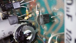
Hi i think this one betterCould you please try to focus on the transistor in question??
Thanks for your help !
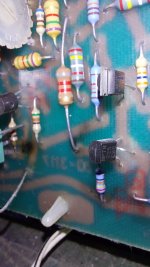
Attachments
Clearly an NPN complementary of 2N4250.

SO: NPN - 40Vce - Hfe 250 to 700 _ TO92 case
Being in "European" Argentina I would use BC547C , maybe others can suggest an "American" type, but in any case BC547 is cheap and plentiful in USA.
Beware of pinout, if it is not an exact match slightly bend legs so they fit in the proper holes.
Replace both TN225 to minimize offset drift.
Hi !Clearly an NPN complementary of 2N4250.
SO: NPN - 40Vce - Hfe 250 to 700 _ TO92 case
Being in "European" Argentina I would use BC547C , maybe others can suggest an "American" type, but in any case BC547 is cheap and plentiful in USA.
Beware of pinout, if it is not an exact match slightly bend legs so they fit in the proper holes.
Replace both TN225 to minimize offset drift.
Thank you very much for the time took to awnser.
I guess I will have to modify them.
Can you tell me what will be the impact of à change in hfe ? Do i have to change the tn225 in right and left channel ?
Thank you for your help !
Please state why are you asking this to begin with.
Are you repairing an amp?
Are you cloning one?
Are you replacing transistors just for the sake of it?
If it works properly as-is, then leave it alone.
Are you repairing an amp?
Are you cloning one?
Are you replacing transistors just for the sake of it?
If it works properly as-is, then leave it alone.
OP mentioned simulation. Probably looking for a model. In another place, the 2N4250 is paired with a 2N5209. That TN225 is probably a selected 2N5209 or similar. In that type of input stage hfe’s should match to minimize input bias current (It would be self-cancelling). For simulation purposes you could probably use 2N5087/2N5210 models which are likely everywhere.
Well I repair this amp to learn how they workPlease state why are you asking this to begin with.
Are you repairing an amp?
Are you cloning one?
Are you replacing transistors just for the sake of it?
If it works properly as-is, then leave it alone.
You can see in the picture that there were some hot points in the amp in the past.
If i succed in repairing it, yes i plan to clone to give a brand new one to my father.
Now the amp is quite unstable, that why I want understand all ils fonctionnement (thanks to simulation) before changing anything.

Perfect I will give a try in simulation thank you !OP mentioned simulation. Probably looking for a model. In another place, the 2N4250 is paired with a 2N5209. That TN225 is probably a selected 2N5209 or similar. In that type of input stage hfe’s should match to minimize input bias current (It would be self-cancelling). For simulation purposes you could probably use 2N5087/2N5210 models which are likely everywhere.
1) maybe simulation does not help you here.
Circuit by itself may be stable, any problems can come from real world layout and grounding.
2) I suggest you clean the schematic using any Graphics software you like (think Photoshop and similar), enlarge drawing 2X and paintbrush or airbrush ugly pots with background colour, so they disappear.
readability will improve immensely.
Long boring work, yet doable in a couple rainy boring Sunday evenings 😉
Here: left was cleaned, right is original, you decide 😉

IF you do it, you can later upload the cleaned schematic 🙂
Circuit by itself may be stable, any problems can come from real world layout and grounding.
2) I suggest you clean the schematic using any Graphics software you like (think Photoshop and similar), enlarge drawing 2X and paintbrush or airbrush ugly pots with background colour, so they disappear.
readability will improve immensely.
Long boring work, yet doable in a couple rainy boring Sunday evenings 😉
Here: left was cleaned, right is original, you decide 😉
IF you do it, you can later upload the cleaned schematic 🙂
🤩🤩😎1) maybe simulation does not help you here.
Circuit by itself may be stable, any problems can come from real world layout and grounding.
2) I suggest you clean the schematic using any Graphics software you like (think Photoshop and similar), enlarge drawing 2X and paintbrush or airbrush ugly pots with background colour, so they disappear.
readability will improve immensely.
Long boring work, yet doable in a couple rainy boring Sunday evenings 😉
Here: left was cleaned, right is original, you decide 😉
View attachment 1102176
IF you do it, you can later upload the cleaned schematic 🙂
God I did not even thought about it ! It is awesome how it is easier to read !1) maybe simulation does not help you here.
Circuit by itself may be stable, any problems can come from real world layout and grounding.
2) I suggest you clean the schematic using any Graphics software you like (think Photoshop and similar), enlarge drawing 2X and paintbrush or airbrush ugly pots with background colour, so they disappear.
readability will improve immensely.
Long boring work, yet doable in a couple rainy boring Sunday evenings 😉
Here: left was cleaned, right is original, you decide 😉
View attachment 1102176
IF you do it, you can later upload the cleaned schematic 🙂
I have drawn the scheme in proteus I still have to put the simulation input (transistor caracteristics)
I will keep you updated !
For now thank you all for your help I think I have everything to continue my investigations !
Have a good Day !
Forget the parts I selected in post #7. For some reason I thought it had to be a 0.5A part?? wg_ski is correct.
I tried to put the schematic pages together but some of it is missing between pages, leaving mysteries in the IPS. It looks like Q13 is a CCS but the transistor connected to R28 is cut off. The ~buffered feedback is very strange and connecting two collectors together in Q5, Q6 is very doubtful.
I tried to put the schematic pages together but some of it is missing between pages, leaving mysteries in the IPS. It looks like Q13 is a CCS but the transistor connected to R28 is cut off. The ~buffered feedback is very strange and connecting two collectors together in Q5, Q6 is very doubtful.
- Home
- Amplifiers
- Solid State
- Can't find old transistor TN225?